
 German
 Japanese
 Portuguese
 Korea
Korea
 Mexico
 Dutch
Dutch


Microchip Technology
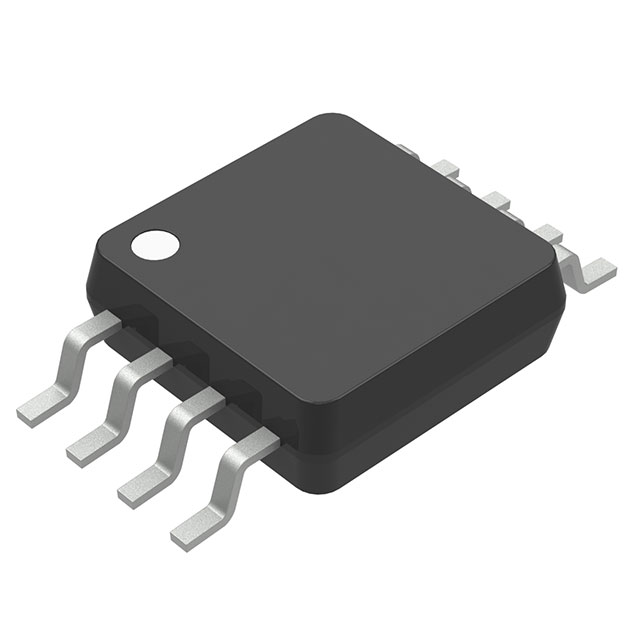
MCP6V12-E/MS

Why Choose Us?
Professional Platform
B2B & B2C purchasingDelivery at full speed
1-2 days deliveryWide variety
Original manufacturers365 days guarantee
Responsible quality
.png)


Tech Specifications
MCP6V12-E/MS Description
MCP6V12-E/MS Description
The MCP6V12-E/MS is a high-performance operational amplifier (op-amp) designed and manufactured by Microchip Technology. This dual-channel, zero-drift op-amp offers a wide supply voltage range from 1.6 V to 5.5 V, making it suitable for a variety of low-voltage applications. With a gain bandwidth product of 80 kHz and a slew rate of 0.03 V/µs, the MCP6V12-E/MS provides excellent performance in demanding signal processing tasks.
MCP6V12-E/MS Features
- Wide Supply Voltage Range: The MCP6V12-E/MS can operate with a supply voltage as low as 1.6 V and as high as 5.5 V, making it ideal for low-voltage applications.
- High Gain Bandwidth Product: With a gain bandwidth product of 80 kHz, the MCP6V12-E/MS offers excellent performance in high-speed signal processing applications.
- Low Input Bias Current: The MCP6V12-E/MS has an ultra-low input bias current of 5 pA, minimizing the loading effect on high-impedance input sources.
- Zero-Drift Technology: The MCP6V12-E/MS utilizes zero-drift technology, ensuring long-term stability and eliminating the need for calibration.
- Low Power Consumption: The MCP6V12-E/MS consumes only 6.5 µA (x2 channels), making it suitable for battery-powered applications.
- High Output Current: Each channel can deliver up to 17 mA, allowing the MCP6V12-E/MS to drive demanding loads.
- Surface Mount Packaging: The MCP6V12-E/MS is available in an 8-pin MSOP package, suitable for surface mount applications.
MCP6V12-E/MS Applications
The MCP6V12-E/MS is ideal for a wide range of applications, including:
- Sensor Signal Conditioning: The low input bias current and zero-drift technology make the MCP6V12-E/MS an excellent choice for conditioning signals from high-impedance sensors.
- Audio Amplification: The wide supply voltage range and low noise performance make the MCP6V12-E/MS suitable for audio amplification applications.
- Battery-Powered Devices: The low power consumption and wide supply voltage range make the MCP6V12-E/MS ideal for battery-powered devices, such as portable instruments and wearable electronics.
- Industrial Control Systems: The MCP6V12-E/MS can be used in industrial control systems where low-voltage operation and high reliability are required.
Conclusion of MCP6V12-E/MS
The MCP6V12-E/MS is a versatile, high-performance op-amp that offers a unique combination of features, including a wide supply voltage range, low input bias current, zero-drift technology, and low power consumption. Its excellent performance in demanding signal processing tasks, combined with its wide range of applications, make the MCP6V12-E/MS an ideal choice for designers looking for a reliable, low-voltage op-amp solution.
FAQ
Not available to buy online? Want the lower wholesale price? Please Send RFQ to get best price, we will respond immediately


.png?x-oss-process=image/format,webp/resize,h_32)


