

Microchip Technology
PIC18F46J50-I/ML
Microcontrollers

Not available to buy online? Want the lower wholesale price? Please Send RFQ to get best price, we will respond immediately


- 1+
- $3.89869
- $3.9
- 10+
- $3.73262
- $37.33
- 30+
- $3.63207
- $108.96
- 100+
- $3.37460
- $337.46

.png?x-oss-process=image/format,webp/resize,p_30)


PIC18F46J50-I/ML Description
Microchip Technology's PIC18F46J50-I/ML is a microcontroller unit (MCU) designed for a wide range of applications. Here is a brief description of the model, its features, and potential applications:
Description:
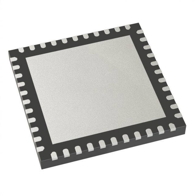
The PIC18F46J50-I/ML is a member of the PIC18F46J50 family of microcontrollers from Microchip Technology. It is an 8-bit flash microcontroller with enhanced mid-range performance and features. The device is housed in a 28-pin, 0.300" (7.62mm) wide, MLP (Micro Lead Frame) package, which is suitable for compact and space-constrained applications.
Features:
- CPU Core: It features a 16-bit instruction set with a wide range of instructions optimized for high code efficiency.
- Memory: The device includes up to 128KB of Flash program memory, 4KB of RAM, and 256 bytes of EEPROM.
- I/O: It has 35 digital I/O lines, which can be used for various input and output functions.
- Timers: It includes up to 7 timers, which can be used for timekeeping, PWM generation, and other timing-related tasks.
- Communication Interfaces: It features a Universal Synchronous/Asynchronous Receiver/Transmitter (USART) for serial communication, a USB interface for high-speed data transfer, and a CAN bus interface for network communication.
- Analog-to-Digital Converter (ADC): It has up to 16 channels of 10-bit ADC, allowing for the conversion of analog signals to digital values.
- Programmable Logic: It includes programmable logic features, such as configurable logic cells (CLC) for custom logic applications.
- Security: The device offers secure features like a unique 64-bit ID, which can be used for authentication and security purposes.
Applications:
The PIC18F46J50-I/ML is suitable for a wide range of applications due to its versatile features and robust performance. Some potential applications include:
- Industrial Control Systems: Its robust timers and communication interfaces make it suitable for use in industrial control systems, such as motor control, sensor interfacing, and process automation.
- Automotive Applications: The device can be used in automotive applications, such as body control modules, lighting control, and engine management systems.
- Consumer Electronics: It can be employed in consumer electronics, like home appliances, gaming devices, and smart home systems.
- Medical Devices: The PIC18F46J50-I/ML can be used in medical devices for monitoring and controlling various parameters, such as blood pressure, heart rate, and temperature.
- Networking Devices: The built-in CAN bus interface makes it suitable for networking devices, such as routers, switches, and IoT gateways.
- Data Acquisition Systems: The device's ADC capabilities make it suitable for data acquisition systems, where it can be used to collect and process analog data from various sensors.
The PIC18F46J50-I/ML's combination of features, performance, and flexibility make it a popular choice for a wide range of embedded systems and applications.
Tech Specifications
PIC18F46J50-I/ML Documents
Download datasheets and manufacturer documentation for PIC18F46J50-I/ML
PIC18F46J50 Family Rev.A2 Errata Assembly Site 22/Nov/2023 PIC18F46J50 Family Packing Changes 10/Oct/2016 Label and Packing Changes 23/Sep/2015 PIC18F46J50 Development Tool Selector Errata/Datasheet Update 07/Aug/2014 Plating 04/Jun/2013 Microchip CA Prop65 Microchip RoHS Microchip REACH Related Parts


Shopping Guide


.png?x-oss-process=image/format,webp/resize,h_32)


©2025 ERSA Electronics Corporation.