
 German
 Japanese
 Portuguese
 Korea
Korea
 Mexico
 Dutch
Dutch


Microchip Technology
PL133-97QC

Why Choose Us?
Professional Platform
B2B & B2C purchasingDelivery at full speed
1-2 days deliveryWide variety
Original manufacturers365 days guarantee
Responsible quality
.png)


Tech Specifications
PL133-97QC Description
PL133-97QC Description
The PL133-97QC is a high-performance clock buffer designed for a wide range of electronic applications. Manufactured by Microchip Technology, this device belongs to the category of Clock/Timing ICs and is specifically engineered provide to reliable and efficient clock signal distribution. The PL133-97QC features a 1:9 fanout buffer configuration, making it ideal for applications requiring multiple clock signal outputs from a single input source.
This IC operates within a temperature range of 0°C to 70°C, ensuring stable performance across various environmental conditions. It supports a supply voltage range of 2.25V to 3.63V, providing flexibility in power supply options. The device is designed with LVCMOS input and output compatibility, allowing seamless integration with a variety of digital systems. The maximum operating frequency of 150 MHz ensures that the PL133-97QC can handle high-speed clock signals, making it suitable for modern, high-performance electronic designs.
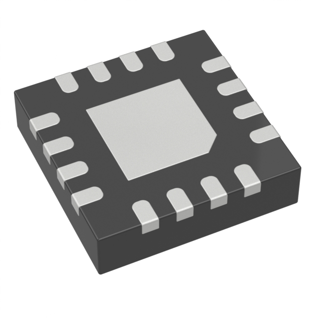
The PL133-97QC is packaged in a 16QFN format, which is ideal for surface mount applications. This packaging choice not only ensures a compact footprint but also enhances thermal performance, which is crucial for high-frequency operations. The device is classified under ECCN EAR99 and HTSUS 8542.39.0001, indicating its compliance with international export regulations and tariff classifications.
PL133-97QC Features
- High Fanout Capability: The 1:9 fanout buffer design allows for efficient distribution of clock signals to multiple destinations, reducing the need for multiple clock sources and simplifying circuit design.
- Wide Operating Temperature Range: With an operating temperature range of 0°C to 70°C, the PL133-97QC ensures reliable performance in various environmental conditions, making it suitable for both industrial and consumer applications.
- Flexible Supply Voltage: The device supports a supply voltage range of 2.25V to 3.63V, providing flexibility in power supply options and compatibility with different system architectures.
- High-Speed Operation: The maximum operating frequency of 150 MHz allows the PL133-97QC to handle high-speed clock signals, making it ideal for applications requiring fast data processing and synchronization.
- LVCMOS Compatibility: The device features LVCMOS input and output compatibility, ensuring seamless integration with a wide range of digital systems and reducing the need for additional level-shifting components.
- Surface Mount Packaging: The 16QFN package format is ideal for surface mount applications, providing a compact footprint and enhanced thermal performance, which is crucial for high-frequency operations.
- Compliance and Safety: The PL133-97QC is REACH unaffected and ROHS3 compliant, ensuring that it meets the highest environmental and safety standards.
PL133-97QC Applications
The PL133-97QC is ideal for a variety of applications where reliable and efficient clock signal distribution is required. Some specific use cases include:
- Telecommunications: In base stations and communication equipment where multiple clock signals are needed for synchronization and data processing.
- Computing: In servers and high-performance computing systems where clock distribution is critical for maintaining system performance and reliability.
- Industrial Automation: In control systems and automation equipment where precise timing and signal distribution are essential for accurate operation.
- Consumer Electronics: In devices such as routers, modems, and smart home systems where clock signals need to be distributed to multiple components.
Conclusion of PL133-97QC
The PL1339-7QC from Microchip Technology is a versatile and high-performance clock buffer designed to meet the demands of modern electronic systems. Its 1:9 fanout buffer configuration, wide operating temperature range, and high-speed operation make it an ideal choice for applications requiring efficient clock signal distribution. The device's LVCMOS compatibility, flexible supply voltage, and surface mount packaging further enhance its suitability for a wide range of applications. With its compliance with international standards and safety regulations, the PL133-97QC ensures reliable performance and environmental responsibility. Whether in telecommunications, computing, industrial automation, or consumer electronics, the PL133-97QC stands out as a reliable and efficient solution for clock signal distribution.
FAQ
| Quantity | Unit Price | Ext. Price |
|---|---|---|
| 1+ | $0.85360 | $0.85 |
| 25+ | $0.71280 | $17.82 |
| 100+ | $0.65120 | $65.12 |
Not available to buy online? Want the lower wholesale price? Please Send RFQ to get best price, we will respond immediately


.png?x-oss-process=image/format,webp/resize,h_32)


