
 German
 Japanese
 Portuguese
 Korea
Korea
 Mexico
 Dutch
Dutch


Microchip Technology
SY89826LHI

Why Choose Us?
Professional Platform
B2B & B2C purchasingDelivery at full speed
1-2 days deliveryWide variety
Original manufacturers365 days guarantee
Responsible quality
.png)


Tech Specifications
SY89826LHI Description
SY89826LHI Description
The SY89826LHI is a high-performance clock buffer designed by Microchip Technology, part of the Precision Edge® series. This device is specifically engineered for applications requiring precise clock distribution and signal translation. It features a 2:22 input-to-output ratio, making it ideal for fanout buffer applications where a single input signal needs to be distributed to multiple outputs. The SY89826LHI supports differential signaling, both for input and output, ensuring high signal integrity and reduced electromagnetic interference (EMI). It operates within a supply voltage range of 3V to 3.6V and is capable of handling frequencies up to 1 GHz, making it suitable for high-speed digital systems.
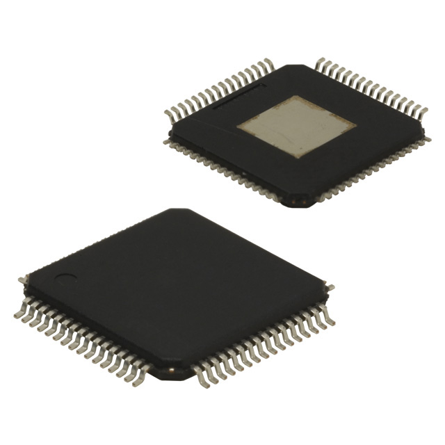
The SY89826LHI is housed in a surface-mount package, specifically a 64-pin TQFP, which is ideal for space-constrained designs. It is categorized under Clock/Timing ICs and is available in bulk packaging. This device is REACH unaffected, ensuring compliance with environmental regulations. Despite its obsolescence status, the SY89826LHI remains a robust choice for legacy systems and applications where its unique features are still highly valued.
SY89826LHI Features
- High-Speed Performance: With a maximum operating frequency of 1 GHz, the SY89826LHI ensures precise clock distribution and minimal signal degradation.
- Differential Signaling: The device supports both LVDS and LVPECL input and LVDS output, providing excellent signal integrity and reduced EMI.
- Flexible Power Supply: Operates within a voltage range of 3V to 3.6V, offering compatibility with a wide range of power supply configurations.
- Surface-Mount Packaging: The 64-pin TQFP package is ideal for compact designs, ensuring ease of integration into modern PCB layouts.
- High Fanout Capability: The 2:22 input-to-output ratio allows for efficient distribution of clock signals to multiple destinations.
- Compliance and Reliability: REACH unaffected status ensures compliance with environmental regulations, while the moisture sensitivity level (MSL) of 3 (168 hours) guarantees reliability in various environmental conditions.
SY89826LHI Applications
The SY89826LHI is well-suited for a variety of high-speed digital applications, including:
- Telecommunications: Ideal for distributing clock signals in telecom equipment, ensuring precise timing and synchronization.
- Data Centers: Used in server and storage systems to distribute clock signals across multiple components, maintaining signal integrity.
- High-Speed Networking: Suitable for networking equipment where high-speed clock distribution is critical for performance.
- Industrial Automation: Provides reliable clock distribution in industrial control systems, ensuring accurate timing and synchronization.
- Consumer Electronics: Used in high-end consumer electronics where precise clock distribution is necessary for optimal performance.
Conclusion of SY89826LHI
The SY89826LHI is a versatile and high-performance clock buffer that offers significant advantages in high-speed digital systems. Its ability to distribute clock signals efficiently, combined with its support for differential signaling and flexible power supply options, makes it a valuable component for a wide range of applications. Despite its obsolescence status, the SY89826LHI remains a reliable choice for legacy systems and applications where its unique features are still highly valued. For designers and engineers looking for a robust clock distribution solution, the SY89826LHI is a compelling option that delivers on performance, reliability, and compliance.
FAQ
Not available to buy online? Want the lower wholesale price? Please Send RFQ to get best price, we will respond immediately


.png?x-oss-process=image/format,webp/resize,h_32)


