
 German
 Japanese
 Portuguese
 Korea
Korea
 Mexico
 Dutch
Dutch


Microchip Technology
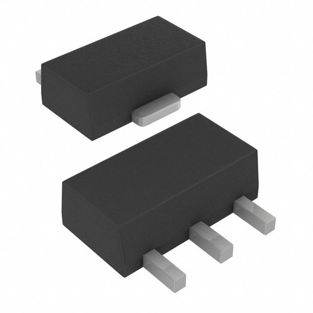
TN0104N8-G

Why Choose Us?
Professional Platform
B2B & B2C purchasingDelivery at full speed
1-2 days deliveryWide variety
Original manufacturers365 days guarantee
Responsible quality
.png)


Tech Specifications
TN0104N8-G Description
TN0104N8-G Description
The TN0104N8-G is a high-performance MOSFET (Metal Oxide) from Microchip Technology, designed for applications requiring robust power management and efficient switching. With its N-CH 40V 630mA TO243AA package, this device offers a combination of high input capacitance, low power dissipation, and a wide range of operating voltages, making it ideal for various electronic systems.
TN0104N8-G Features
- Input Capacitance (Ciss): The TN0104N8-G boasts a maximum input capacitance of 70 pF at 20 V, ensuring fast switching and minimal signal distortion.
- Drain to Source Voltage (Vdss): Capable of withstanding 40 V, this MOSFET can handle high voltage applications with ease.
- Power Dissipation: With a maximum power dissipation of 1.6W (Tc), the TN0104N8-G is designed for efficient operation in various power-sensitive environments.
- Technology: Utilizing advanced MOSFET technology, this device offers superior performance and reliability.
- Rds On (Max): The TN0104N8-G has a maximum Rds On of 2 Ohms at 1A, 10V, ensuring low resistance and high efficiency in conduction.
- Vgs(th) (Max): The threshold voltage is a maximum of 1.6V at 500µA, providing excellent control over the device's operation.
- Current - Continuous Drain (Id): Capable of handling 630mA at 25°C, this MOSFET is suitable for applications requiring high current flow.
TN0104N8-G Applications
The TN0104N8-G is ideal for a variety of applications, including:
- Power Management: Due to its high voltage and current capabilities, this MOSFET is perfect for managing power in electronic devices.
- Switching Applications: The low Rds On and high input capacitance make it an excellent choice for switching applications where efficiency and speed are crucial.
- Automotive Electronics: The TN0104N8-G's robust design and performance make it suitable for use in automotive electronics, where reliability and durability are essential.
Conclusion of TN0104N8-G
The TN0104N8-G from Microchip Technology is a versatile and powerful MOSFET, offering a unique combination of high input capacitance, low power dissipation, and a wide range of operating voltages. Its advanced technology and robust design make it an ideal choice for a variety of applications, including power management, switching, and automotive electronics. With its unique features and advantages over similar models, the TN0104N8-G is a reliable and efficient solution for demanding electronic systems.
FAQ
Not available to buy online? Want the lower wholesale price? Please Send RFQ to get best price, we will respond immediately


.png?x-oss-process=image/format,webp/resize,h_32)


