
 German
 Japanese
 Portuguese
 Korea
Korea
 Mexico
 Dutch
Dutch


Microchip Technology
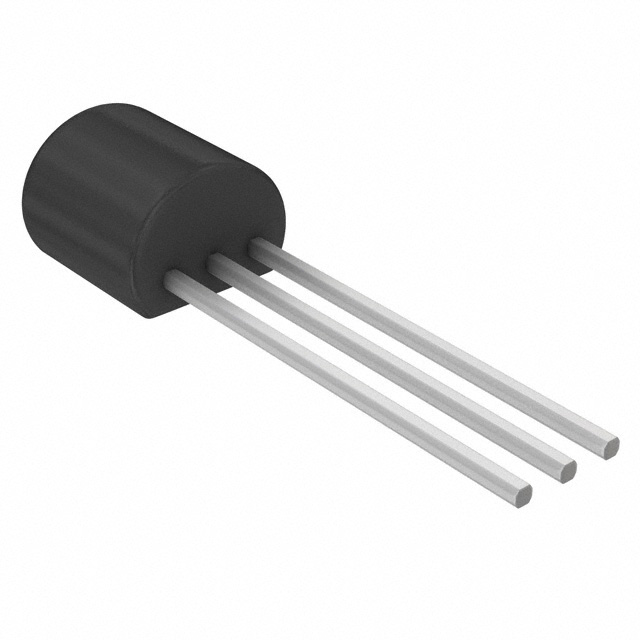
TP0604N3-G

Why Choose Us?
Professional Platform
B2B & B2C purchasingDelivery at full speed
1-2 days deliveryWide variety
Original manufacturers365 days guarantee
Responsible quality
.png)


Tech Specifications
TP0604N3-G Description
TP0604N3-G Description
The TP0604N3-G from Microchip Technology is a P-Channel MOSFET designed for efficient power management in low-voltage applications. With a drain-to-source voltage (Vdss) rating of 40V and a continuous drain current (Id) of 430mA, this device is optimized for compact, energy-efficient designs. Its low input capacitance (Ciss) of 150pF @ 20V ensures fast switching performance, while the maximum Rds(on) of 2Ω @ 1A, 10V minimizes conduction losses. The MOSFET operates with a gate threshold voltage (Vgs(th)) as low as 2.4V @ 1mA, making it compatible with low-drive-voltage circuits. Packaged in a TO-92-3 through-hole format, it is suitable for prototyping and industrial applications requiring reliable through-hole mounting.
TP0604N3-G Features
- Low Rds(on): 2Ω @ 1A, 10V for reduced power dissipation.
- Fast Switching: Low input capacitance (150pF) enhances high-frequency performance.
- Wide Vgs Range: Supports ±20V, offering flexibility in gate drive design.
- High Efficiency: Optimized for low-voltage operation (drive voltage: 5V–10V).
- Robust Construction: TO-92-3 package ensures mechanical durability.
- Compliance: ROHS3 Compliant, REACH Unaffected, and MSL 1 (Unlimited) for environmental and handling reliability.
- Low Threshold Voltage: 2.4V @ 1mA enables compatibility with logic-level signals.
TP0604N3-G Applications
- Power Management: Ideal for DC-DC converters, load switches, and battery protection circuits due to low Rds(on) and efficient switching.
- Portable Electronics: Suitable for low-power devices such as handheld instruments, where space and energy efficiency are critical.
- Automotive Systems: Used in low-voltage automotive modules (e.g., sensors, lighting) thanks to its 40V rating and reliability.
- Industrial Controls: Deployed in relay drivers and motor control circuits requiring through-hole mounting.
- Consumer Electronics: Fits power-saving modes in appliances and peripherals.
Conclusion of TP0604N3-G
The TP0604N3-G stands out as a high-performance P-Channel MOSFET for low-power, high-efficiency applications. Its low conduction losses, fast switching, and robust TO-92-3 package make it a versatile choice for designers prioritizing reliability and compactness. With compliance to environmental standards and broad applicability in automotive, industrial, and consumer electronics, this MOSFET is a dependable solution for modern power management challenges.
FAQ
Not available to buy online? Want the lower wholesale price? Please Send RFQ to get best price, we will respond immediately


.png?x-oss-process=image/format,webp/resize,h_32)


