
 German
 Japanese
 Portuguese
 Korea
Korea
 Mexico
 Dutch
Dutch


Microchip Technology
VP3203N8-G

Why Choose Us?
Professional Platform
B2B & B2C purchasingDelivery at full speed
1-2 days deliveryWide variety
Original manufacturers365 days guarantee
Responsible quality
.png)


Tech Specifications
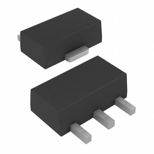
VP3203N8-G Description
VP3203N8-G Description
The VP3203N8-G from Microchip Technology is a P-Channel MOSFET designed for high-efficiency power management applications. With a 30V drain-to-source voltage (Vdss) and 1.1A continuous drain current (Id), this device is optimized for low-power switching and load control. It features a low on-resistance (Rds(on)) of 600mΩ at 1.5A and 10V gate drive, ensuring minimal conduction losses. The MOSFET operates with a gate threshold voltage (Vgs(th)) of 3.5V (max) at 10mA, making it compatible with standard logic-level drive circuits. Packaged in a TO-243AA (SOT-89) surface-mount form factor, it is suitable for space-constrained designs.
VP3203N8-G Features
- Low Input Capacitance: 300pF (max) at 25V reduces switching losses, improving efficiency in high-frequency applications.
- Wide Gate Drive Range: Supports ±20V Vgs (max), enhancing flexibility in various drive conditions.
- Power Efficiency: 1.6W max power dissipation (Ta) ensures reliable thermal performance in compact designs.
- Robust Construction: ROHS3 Compliant and REACH Unaffected, meeting stringent environmental standards.
- Reliability: MSL 1 (Unlimited) moisture sensitivity rating ensures long shelf life and ease of handling.
- Optimized Drive Voltage: Operates efficiently at 4.5V to 10V gate drive, balancing performance and power consumption.
VP3203N8-G Applications
- Battery Management: Ideal for load switching and reverse polarity protection in portable devices.
- Power Distribution: Used in DC-DC converters and voltage regulation circuits due to low Rds(on).
- Signal Switching: Suitable for analog/digital multiplexing in low-voltage systems.
- Consumer Electronics: Commonly deployed in smartphones, wearables, and IoT devices for power gating.
- Industrial Controls: Reliable performance in motor drivers and solenoid control applications.
Conclusion of VP3203N8-G
The VP3203N8-G stands out as a high-performance P-Channel MOSFET, offering low on-resistance, efficient switching, and compact packaging. Its wide gate drive tolerance and low power dissipation make it a versatile choice for modern electronics. Whether in battery-powered systems, power management, or industrial controls, this MOSFET delivers reliable operation and energy efficiency, making it a preferred solution for engineers seeking optimized performance in constrained spaces.
FAQ
Not available to buy online? Want the lower wholesale price? Please Send RFQ to get best price, we will respond immediately


.png?x-oss-process=image/format,webp/resize,h_32)


