
 German
 Japanese
 Portuguese
 Korea
Korea
 Mexico
 Dutch
Dutch


Microchip Technology
ZL40252LDF1

Why Choose Us?
Professional Platform
B2B & B2C purchasingDelivery at full speed
1-2 days deliveryWide variety
Original manufacturers365 days guarantee
Responsible quality
.png)


Tech Specifications
ZL40252LDF1 Description
ZL40252LDF1 Description
The ZL40252LDF1 is a high-performance clock buffer from Microchip Technology, designed to provide reliable and efficient signal distribution in a wide range of electronic systems. This device is part of the SmartBuffer™ series, known for its advanced features and robust performance. The ZL40252LDF1 features a 4:10 input-to-output ratio, making it ideal for applications requiring multiple output signals from a single input source. It supports differential signaling on both input and output, ensuring high signal integrity and reduced electromagnetic interference (EMI).
The ZL40252LDF1 operates over a wide supply voltage range of 1.71V to 3.465V, providing flexibility in power supply design. It supports various input types, including CMOS and crystal, and offers a comprehensive range of output formats such as CML, CMOS, HCSL, HSTL, LVDS, LVPECL, and SSTL. This versatility makes it suitable for diverse applications, from high-speed digital systems to precision timing circuits.
ZL40252LDF1 Features
- High Frequency Performance: The ZL40252LDF1 supports a maximum operating frequency of 1.035 GHz, ensuring it can handle high-speed clock signals with minimal jitter and phase noise.
- Differential Signaling: Both input and output support differential signaling, which enhances signal integrity and reduces susceptibility to noise and interference.
- Versatile Output Formats: The device supports multiple output formats, including CML, CMOS, HCSL, HSTL, LVDS, LVPECL, and SSTL, providing flexibility in system design.
- Wide Supply Voltage Range: Operates from 1.71V to 3.465V, offering compatibility with various power supply configurations.
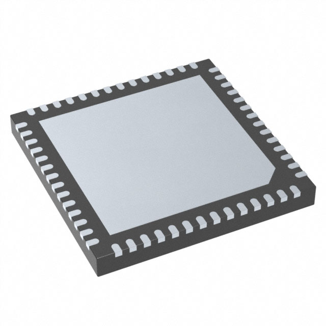
- Surface Mount Packaging: The ZL40252LDF1 is available in a surface mount package, specifically a 56-pin QFN, which is ideal for compact and high-density PCB designs.
- Compliance and Reliability: The device is REACH unaffected and RoHS3 compliant, ensuring it meets environmental and safety standards. It also has a moisture sensitivity level (MSL) of 3, making it suitable for standard manufacturing processes.
ZL40252LDF1 Applications
The ZL40252LDF1 is ideal for a variety of applications where high-speed clock distribution and signal integrity are critical. Some specific use cases include:
- High-Speed Digital Systems: Ideal for distributing clock signals in high-speed digital systems such as FPGAs, ASICs, and high-performance computing platforms.
- Telecommunications: Suitable for use in telecommunications infrastructure, where precise timing and low jitter are essential for data transmission.
- Industrial Automation: Provides reliable clock distribution in industrial automation systems, ensuring accurate timing for control and monitoring applications.
- Consumer Electronics: Can be used in consumer electronics such as high-definition displays and multimedia devices, where high-speed signal distribution is required.
Conclusion of ZL40252LDF1
The ZL40252LDF1 from Microchip Technology is a versatile and high-performance clock buffer that offers significant advantages over similar models. Its wide range of supported input and output formats, differential signaling capabilities, and high operating frequency make it an excellent choice for a variety of applications. The device's compliance with environmental and safety standards, along with its robust packaging and reliability, further enhance its appeal. Whether used in high-speed digital systems, telecommunications, industrial automation, or consumer electronics, the ZL40252LDF1 provides reliable and efficient clock distribution, ensuring optimal system performance.
FAQ
Not available to buy online? Want the lower wholesale price? Please Send RFQ to get best price, we will respond immediately


.png?x-oss-process=image/format,webp/resize,h_32)


