

Micron Technology
JS28F512P33BFD
Memory ICs Products

Not available to buy online? Want the lower wholesale price? Please Send RFQ to get best price, we will respond immediately


.png?x-oss-process=image/format,webp/resize,p_30)


JS28F512P33BFD Description
JS28F512P33BFD Description
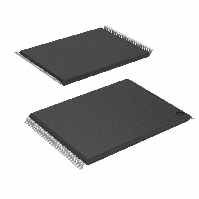
The JS28F512P33BFD is a 512Mbit parallel flash memory device from Micron Technology Inc., designed for high-performance applications. With a clock frequency of 40 MHz and an access time of 105 ns, this memory IC offers fast data retrieval and processing capabilities. The device is packaged in a 56-pin TSOP (Thin Shrink Small Outline Package) and is surface-mountable, making it suitable for space-constrained applications. The JS28F512P33BFD operates over a wide voltage range of 2.3V to 3.6V and is compliant with the RoHS3 standard, ensuring environmental friendliness.
JS28F512P33BFD Features
- Memory Format: FLASH, providing non-volatile storage for data retention even in the absence of power.
- Memory Interface: Parallel, allowing for high-speed data transfer and compatibility with a wide range of systems.
- Memory Organization: 32M x 16, offering a large storage capacity for various applications.
- Write Cycle Time: 105 ns for both word and page writes, ensuring fast data input.
- Voltage - Supply: 2.3V ~ 3.6V, providing flexibility in power supply requirements.
- Access Time: 105 ns, enabling rapid data access.
- Moisture Sensitivity Level (MSL): 3 (168 Hours), indicating the device's resistance to moisture-induced damage.
- REACH Status: REACH Unaffected, ensuring compliance with European chemical regulations.
- ECCN: 3A991B1A, facilitating international trade and export.
- HTSUS: 8542.32.0071, simplifying customs and import processes.
JS28F512P33BFD Applications
The JS28F512P33BFD is ideal for applications requiring high-speed data storage and retrieval, such as:
- Industrial Control Systems: Due to its fast access time and write cycle, it can be used for storing and processing control algorithms and system parameters.
- Automotive Infotainment Systems: The device's ability to withstand harsh conditions, such as temperature fluctuations and vibrations, makes it suitable for automotive applications.
- Embedded Systems: The JS28F512P33BFD can be used for storing firmware, operating systems, and application data in embedded systems, such as IoT devices and smart home appliances.
- Data Logging and Recording: The large storage capacity and fast write times make it suitable for applications that require logging and recording large amounts of data, such as in medical devices or security systems.
Conclusion of JS28F512P33BFD
The JS28F512P33BFD is a high-performance, non-volatile memory IC from Micron Technology Inc., offering fast data access and processing capabilities. Its unique features, such as a wide voltage range, RoHS3 compliance, and REACH unaffected status, make it suitable for a variety of applications, including industrial control systems, automotive infotainment, embedded systems, and data logging. Despite its obsolete status, the JS28F512P33BFD remains a reliable choice for applications requiring high-speed data storage and retrieval.
Tech Specifications
JS28F512P33BFD Documents
Download datasheets and manufacturer documentation for JS28F512P33BFD
Tray Pkg Label Chgs 8/Oct/2020 P33-65nm Standard Pkg Label Chg 20/Feb/2019 Label 12/Sep/2016 P33-65nm Related Parts


Relevant Search
Shopping Guide


.png?x-oss-process=image/format,webp/resize,h_32)


©2025 ERSA Electronics Corporation.