
 German
 Japanese
 Portuguese
 Korea
Korea
 Mexico
 Dutch
Dutch


Why Choose Us?
Professional Platform
B2B & B2C purchasingDelivery at full speed
1-2 days deliveryWide variety
Original manufacturers365 days guarantee
Responsible quality
.png)


Tech Specifications
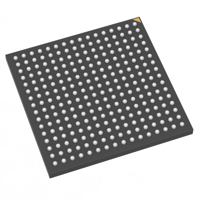
A3P250L-1FGG256I Description
Microsemi's A3P250L-1FGG256I is a high-performance, low-power, and highly integrated FPGA (Field Programmable Gate Array) device. It belongs to the PolarFire family of FPGAs, which are designed to provide exceptional performance and power efficiency for a wide range of applications.
Description:
The A3P250L-1FGG256I is a mid-range FPGA that offers a balance between performance, power consumption, and cost. It features a compact 256-ball fine-pitch ball grid array (FBGA) package, making it suitable for applications with space constraints. The device has a total of 250,000 logic elements (LEs) and 1,024 embedded memory blocks, providing ample resources for complex designs.
Features:
- Low Power Consumption: The PolarFire FPGAs are designed with a focus on low power consumption, making them ideal for battery-powered or energy-sensitive applications.
- High Performance: The A3P250L-1FGG256I offers high-performance capabilities with its advanced 12 nm FinFET technology, enabling faster processing and improved system performance.
- Security Features: The device includes advanced security features, such as hardware-based encryption and secure boot, to protect intellectual property and ensure data integrity.
- Integrated Memory: The FPGA comes with 1,024 embedded memory blocks, providing ample resources for complex designs and reducing the need for external memory components.
- High I/O Count: The A3P250L-1FGG256I has a high I/O count, supporting a wide range of peripherals and interfaces.
- Configuration and Debugging: The device supports JTAG and SPI configuration interfaces, as well as advanced debugging features, making it easier to develop and debug designs.
Applications:
The A3P250L-1FGG256I is suitable for a wide range of applications, including:
- Industrial Automation: The FPGA's low power consumption and high performance make it ideal for industrial control systems and automation equipment.
- Communication Systems: The device's high I/O count and support for various communication protocols make it suitable for communication systems, such as base stations and routers.
- Automotive: The A3P250L-1FGG256I can be used in various automotive applications, such as infotainment systems, advanced driver assistance systems (ADAS), and powertrain control.
- Aerospace and Defense: The FPGA's security features and high reliability make it suitable for aerospace and defense applications, such as satellite communication systems and radar processing.
- Medical Electronics: The device's compact form factor and low power consumption make it suitable for medical electronics, such as imaging systems and patient monitoring devices.
- Consumer Electronics: The A3P250L-1FGG256I can be used in consumer electronics, such as smart home devices, wearables, and IoT applications.
FAQ
Not available to buy online? Want the lower wholesale price? Please Send RFQ to get best price, we will respond immediately


.png?x-oss-process=image/format,webp/resize,h_32)


