
 German
 Japanese
 Portuguese
 Korea
Korea
 Mexico
 Dutch
Dutch


Microsemi
M2S050S-1FGG484I

Why Choose Us?
Professional Platform
B2B & B2C purchasingDelivery at full speed
1-2 days deliveryWide variety
Original manufacturers365 days guarantee
Responsible quality
.png)


Tech Specifications
M2S050S-1FGG484I Description
M2S050S-1FGG484I Description
The M2S050S-1FGG484I is a highly integrated System on Chip (SoC) from Microsemi Corporation, part of the SmartFusion®2 series. This SoC combines a Cortex-M3 microcontroller (MCU) with a field-programmable gate array (FPGA) architecture, offering a powerful and flexible solution for a wide range of embedded applications. The device operates at a clock speed of 166MHz, providing high-performance processing capabilities. It features 256KB of flash memory and 64KB of RAM, ensuring ample storage and fast data access for complex applications. The M2S050S-1FGG484I also supports a comprehensive set of peripherals, including DDR, PCIe, and SERDES, making it suitable for advanced communication and data processing tasks.
M2S050S-1FGG484I Features
- High-Speed Performance: With a clock speed of 166MHz, the M2S050S-1FGG484I delivers rapid processing capabilities, ideal for real-time applications.
- Dual Architecture: The combination of an MCU and FPGA allows for both deterministic control and flexible logic implementation, enhancing overall system functionality.
- Robust Memory: 256KB of flash memory and 64KB of RAM provide sufficient storage for firmware and data, supporting complex algorithms and large datasets.
- Extensive Connectivity: The SoC supports multiple communication protocols, including CANbus, Ethernet, I2C, SPI, UART/USART, and USB, facilitating seamless integration into various systems.
- Advanced Peripherals: Integration of DDR, PCIe, and SERDES peripherals enables high-speed data transfer and connectivity to external devices.
- High I/O Count: With 267 I/O pins, the M2S050S-1FGG484I offers extensive connectivity options, making it suitable for applications requiring multiple interfaces.
- Compliance and Safety: The device is REACH unaffected and classified under ECCN 5A002A1, ensuring compliance with international regulations.
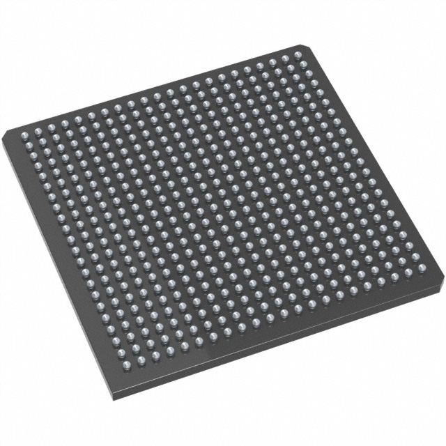
- Packaging and Sensitivity: The M2S050S-1FGG484I is packaged in a 484-pin BGA format and has a moisture sensitivity level (MSL) of 3, suitable for standard manufacturing processes.
M2S050S-1FGG484I Applications
The M2S050S-1FGG484I is ideal for applications requiring high performance, flexibility, and extensive connectivity. Its dual architecture makes it suitable for:
- Industrial Automation: The combination of MCU and FPGA allows for precise control and real-time processing, essential for industrial control systems.
- Communication Systems: The wide range of connectivity options and high-speed peripherals make it ideal for networking equipment and communication gateways.
- Medical Devices: The device's high reliability and extensive I/O capabilities are well-suited for medical monitoring and diagnostic equipment.
- Automotive Systems: The robust connectivity and processing power support advanced driver assistance systems (ADAS) and in-vehicle infotainment (IVI) systems.
- Consumer Electronics: The SoC's flexibility and high performance make it a good fit for smart home devices, gaming consoles, and other consumer electronics.
Conclusion of M2S050S-1FGG484I
The M2S050S-1FGG484I from Microsemi Corporation is a versatile and powerful SoC that combines the benefits of a Cortex-M3 MCU with an FPGA, offering high performance and extensive connectivity options. Its 166MHz clock speed, 256KB of flash memory, and 64KB of RAM provide robust processing and storage capabilities. The device's extensive I/O count and support for multiple communication protocols make it suitable for a wide range of applications, from industrial automation to consumer electronics. Although the product is now obsolete, its unique features and capabilities continue to make it a valuable component for existing systems and legacy designs.
FAQ
Not available to buy online? Want the lower wholesale price? Please Send RFQ to get best price, we will respond immediately


.png?x-oss-process=image/format,webp/resize,h_32)


