
 German
 Japanese
 Portuguese
 Korea
Korea
 Mexico
 Dutch
Dutch


Nexperia
74ABT00DB,112

Why Choose Us?
Professional Platform
B2B & B2C purchasingDelivery at full speed
1-2 days deliveryWide variety
Original manufacturers365 days guarantee
Responsible quality
.png)


Tech Specifications
74ABT00DB,112 Description
74ABT00DB,112 Description
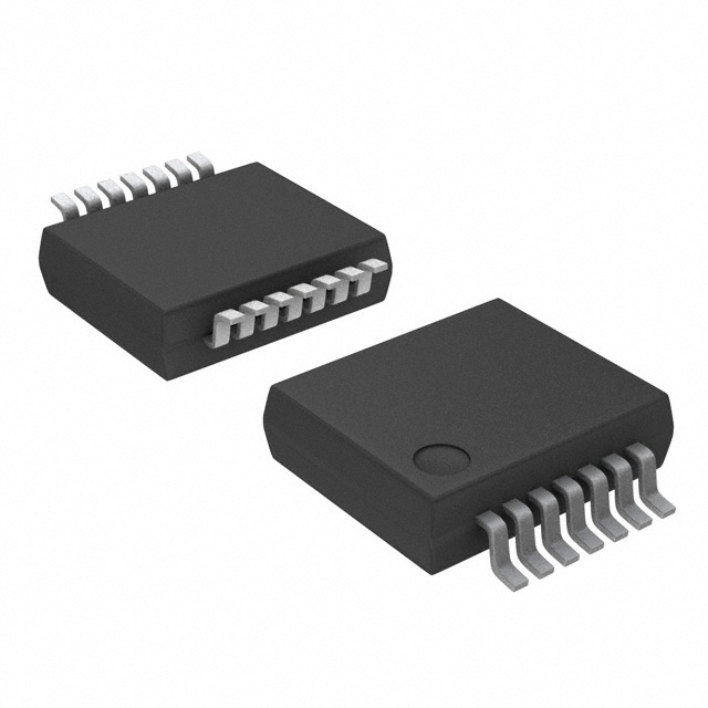
The 74ABT00DB,112 is a high-performance NAND gate logic IC chip, designed for a wide range of digital applications. Manufactured by Nexperia USA Inc., this device is part of the 74ABT series, known for its robust performance and reliability. The 74ABT00DB,112 features a surface mount package, making it suitable for compact and space-efficient designs. It operates within a supply voltage range of 4.5V to 5.5V and offers a maximum propagation delay of 3.6ns at 5V with a load capacitance of 50pF. This IC is equipped with four NAND gates, each with two inputs, providing a versatile solution for digital logic circuits.
74ABT00DB,112 Features
- Logic Type: NAND Gate
- Number of Circuits: 4
- Number of Inputs per Circuit: 2-
Max Propagation Delay: 3.6ns @ 5V, 50pF - Supply Voltage Range: 4.5V ~ 5.5V
- Input Logic Levels: Low (0.8V), High (2V)
- Output Current: High (15mA), Low (20mA)
- Quiescent Current: Max 50 µA
- Mounting Type: Surface Mount
- Package: Tube
- Moisture Sensitivity Level (MSL): 1 (Unlimited)
- Compliance: ROHS3 Compliant, REACH Unaffected
- ECCN: EAR99
- HTSUS: 8542.39.0001
The 74ABT00DB,112 stands out for its low propagation delay, making it ideal for high-speed digital applications. Its surface mount package ensures ease of integration into modern circuit designs. The device's compliance with industry standards such as ROHS3 and REACH ensures it is suitable for a wide range of applications without environmental concerns.
74ABT00DB,112 Applications
The 74ABT00DB,112 is well-suited for a variety of applications where high-speed digital logic is required. Its low propagation delay and robust performance make it ideal for use in:
- Digital Signal Processing: Efficiently processing digital signals in real-time applications.
- Control Systems: Implementing complex control algorithms with minimal delay.
- Data Communication: Managing data flow in high-speed communication systems.
- ** ElectronicsConsumer**: Enhancing the performance of digital circuits in consumer devices.
- Industrial Automation: Providing reliable logic control in industrial environments.
Conclusion of 74ABT00DB,112
The 74ABT00DB,112 is a versatile and high-performance NAND gate IC, offering significant advantages in terms of speed, reliability, and ease of integration. Its low propagation delay and surface mount package make it an excellent choice for modern digital circuit designs. Despite being marked as obsolete, the 74ABT00DB,112 remains a reliable option for applications requiring robust digital logic. Its compliance with industry standards ensures it meets environmental and safety requirements, making it a trustworthy component for a wide range of applications.
FAQ
Not available to buy online? Want the lower wholesale price? Please Send RFQ to get best price, we will respond immediately


.png?x-oss-process=image/format,webp/resize,h_32)


