
 German
 Japanese
 Portuguese
 Korea
Korea
 Mexico
 Dutch
Dutch


Nexperia
74HC4049PW,118

Why Choose Us?
Professional Platform
B2B & B2C purchasingDelivery at full speed
1-2 days deliveryWide variety
Original manufacturers365 days guarantee
Responsible quality
.png)


Tech Specifications
74HC4049PW,118 Description
74HC4049PW,118 Description
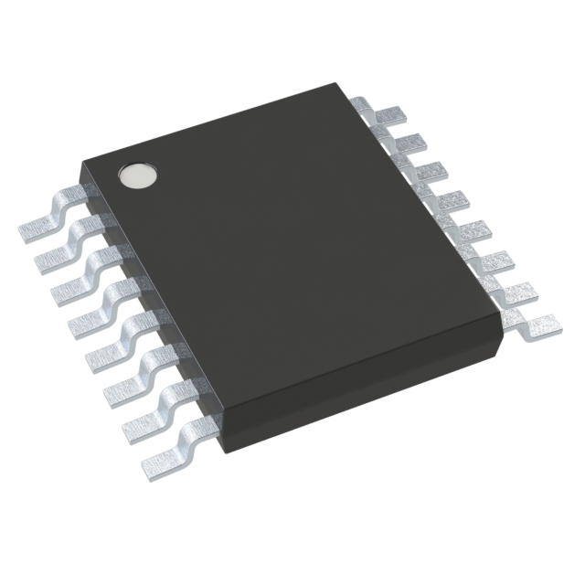
The 74HC4049PW,118 is a high-performance logic IC chip manufactured by Nexperia USA Inc., designed to provide robust buffering and inverting capabilities in a compact 16TSSOP package. This device is part of the widely recognized 74HC series, known for its reliability and versatility in digital circuit applications. The 74HC4049PW,118 features six independent inverting buffers, each capable of handling one bit of data, making it an ideal component for signal processing and logic level conversion tasks.
74HC4049PW,118 Features
- High Performance and Reliability: The 74HC4049PW,118 operates within a wide voltage range of 2V to 6V, ensuring compatibility with various power supply configurations. This flexibility makes it suitable for a broad range of applications, from low-power embedded systems to high-voltage industrial controls.
- Inverting Buffers: Each of the six buffers inverts the input signal, providing a logical NOT function. This feature is particularly useful in digital circuits where signal inversion is required for synchronization, noise reduction, or logic level conversion.
- High Current Capability: With an output current capacity of 5.2mA for both high and low states, the 74HC4049PW,118 can drive multiple loads or interface with other digital components without significant voltage drop or signal degradation.
- Surface Mount Technology (SMT): The surface mount package allows for efficient PCB design and assembly, reducing the overall footprint and improving thermal performance. The 16TSSOP package is well-suited for automated manufacturing processes, ensuring high reliability and consistent performance.
- Compliance and Safety: The 74HC4049PW,118 is REACH unaffected and RoHS3 compliant, adhering to stringent environmental and safety standards. This compliance ensures that the device is suitable for use in environmentally conscious applications and meets regulatory requirements for electronic components.
- Moisture Sensitivity Level (MSL): With an MSL rating of 1 (Unlimited), the 74HC4049PW,118 is highly resistant to moisture, making it ideal for use in humid or challenging environmental conditions without the need for special handling or storage precautions.
74HC4049PW,118 Applications
The 74HC4049PW,118 is a versatile component suitable for a wide range of applications, including:
- Digital Signal Processing: Ideal for inverting and buffering digital signals in microcontroller-based systems, ensuring clean and reliable signal transmission.
- Logic Level Conversion: Useful in applications where signal levels need to be converted or adapted, such as interfacing between different voltage level systems.
- Noise Reduction: By providing a clean, inverted signal, the 74HC4049PW,118 helps reduce noise and improve signal integrity in digital circuits.
- Synchronization: Inverting buffers can be used to synchronize signals in complex digital systems, ensuring proper timing and coordination between different components.
- Industrial Controls: The wide operating voltage range and high current capability make the 74HC4049PW,118 suitable for industrial applications where robustness and reliability are critical.
Conclusion of 74HC4049PW,118
The 74HC4049PW,118 stands out as a reliable and versatile logic IC chip, offering high performance and a wide range of features that make it suitable for various digital circuit applications. Its ability to invert and buffer signals, combined with its robustness and compliance with environmental standards, positions it as an excellent choice for engineers and designers working on complex digital systems. Whether used in signal processing, logic level conversion, or noise reduction, the 74HC4049PW,118 provides a reliable and efficient solution, ensuring optimal performance and reliability in a compact and easy-to-manufacture package.
FAQ
| Quantity | Unit Price | Ext. Price |
|---|---|---|
| 1+ | $0.37840 | $0.38 |
| 10+ | $0.26312 | $2.63 |
| 50+ | $0.21648 | $10.82 |
| 100+ | $0.20187 | $20.19 |
| 2500+ | $0.16152 | $403.80 |
Not available to buy online? Want the lower wholesale price? Please Send RFQ to get best price, we will respond immediately


.png?x-oss-process=image/format,webp/resize,h_32)


