
 German
 Japanese
 Portuguese
 Korea
Korea
 Mexico
 Dutch
Dutch


Nexperia
74HC4051DB,112

Why Choose Us?
Professional Platform
B2B & B2C purchasingDelivery at full speed
1-2 days deliveryWide variety
Original manufacturers365 days guarantee
Responsible quality
.png)


Tech Specifications
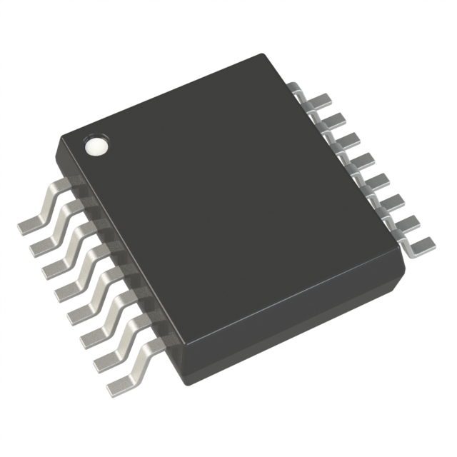
74HC4051DB,112 Description
74HC4051DB,112 Description
The 74HC4051DB,112 is an 8:1 multiplexer/demultiplexer integrated circuit designed for high-performance signal routing in various electronic systems. Manufactured by Nexperia USA Inc., this IC offers a robust and versatile solution for applications requiring efficient signal switching and routing. Despite being marked as obsolete, the 74HC4051DB,112 remains a reliable choice for engineers and designers due to its comprehensive feature set and performance capabilities.
74HC4051DB,112 Features
- Multiplexer/Demultiplexer Circuit: The 74HC4051DB,112 features an 8:1 multiplexer/demultiplexer circuit, allowing for the selection of one of eight input signals to be routed to a single output or vice versa.
- On-State Resistance: With a maximum on-state resistance (Ron) of 120 ohms, this IC ensures minimal signal attenuation and power loss, making it suitable for high-efficiency signal switching.
- Channel-to-Channel Matching: The channel-to-channel matching (ΔRon) is tightly controlled at 6 ohms, ensuring consistent performance across all channels.
- Channel Capacitance: The channel capacitance (CS(off), CD(off)) is a low 3.5 pF, contributing to fast switching times and minimal signal distortion.
- Switch Time: The switch time (Ton, Toff) is exceptionally fast at 51 ns and 42 ns respectively, enabling high-speed signal routing.
- Supply Voltage Range: The IC operates over a wide supply voltage range, from ±1.5V to ±5V for dual supply and 2V to 10V for single supply, providing flexibility in power requirements.
- Bandwidth: The -3dB bandwidth of 180 MHz ensures high-frequency signal integrity, making it ideal for applications requiring high-speed data transmission.
- Compliance: The 74HC4051DB,112 is REACH unaffected and RoHS3 compliant, adhering to stringent environmental and safety standards.
- Leakage Current: The maximum leakage current (IS(off)) is a low 400 nA, ensuring minimal power consumption and signal degradation when the channels are off.
- Moisture Sensitivity Level: With a moisture sensitivity level (MSL) of 1 (unlimited), the IC is highly resistant to moisture, enhancing reliability in various environmental conditions.
- Packaging: The IC is available in a tube package, facilitating easy handling and integration into surface-mount designs.
74HC4051DB,112 Applications
The 74HC4051DB,112 is well-suited for a variety of applications where efficient signal routing and switching are critical. Some specific use cases include:
- Data Acquisition Systems: Ideal for routing multiple analog signals to a single analog-to-digital converter (ADC) input, enhancing the efficiency and accuracy of data acquisition.
- Test and Measurement Equipment: Enables the selection and routing of various input signals to measurement devices, facilitating versatile and precise testing.
- Communication Systems: Suitable for high-speed signal switching in communication systems, ensuring minimal signal delay and distortion.
- Industrial Control Systems: Provides reliable signal routing for control signals in industrial applications, contributing to efficient and accurate control mechanisms.
- Medical Devices: Ensures high reliability and signal integrity in medical devices requiring precise signal switching and routing.
Conclusion of 74HC4051DB,112
The 74HC4051DB,112 is a versatile and high-performance multiplexer/demultiplexer IC that offers significant advantages over similar models. Its low on-state resistance, fast switch times, and wide supply voltage range make it an ideal choice for applications requiring efficient signal routing and switching. Despite being marked as obsolete, its robust feature set and compliance with environmental standards ensure its continued relevance in the electronics industry. For engineers and designers seeking a reliable and efficient solution for signal switching, the 74HC4051DB,112 remains a compelling option.
FAQ
| Quantity | Unit Price | Ext. Price |
|---|---|---|
| 329+ | $0.80080 | $263.46 |
Not available to buy online? Want the lower wholesale price? Please Send RFQ to get best price, we will respond immediately


.png?x-oss-process=image/format,webp/resize,h_32)


