
 German
 Japanese
 Portuguese
 Korea
Korea
 Mexico
 Dutch
Dutch


Nexperia
74HCT132DB,118

Why Choose Us?
Professional Platform
B2B & B2C purchasingDelivery at full speed
1-2 days deliveryWide variety
Original manufacturers365 days guarantee
Responsible quality
.png)


Tech Specifications
74HCT132DB,118 Description
74HCT132DB,118 Description
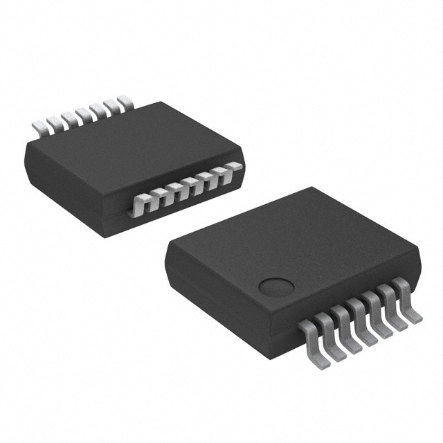
The 74HCT132DB,118 is a NAND gate IC featuring four channels with two inputs each, designed for surface mount applications. Manufactured by Nexperia USA Inc., this IC belongs to the 74HCT series and is housed in a 14-pin small outline package (14SSOP). It operates within a supply voltage range of 4.5V to 5.5V and offers a maximum propagation delay of 33ns at 4.5V with a load capacitance of 50pF. The input logic levels are specified as 0.5V to 0.6V for low and 1.9V to 2.1V for high, ensuring compatibility with a variety of digital circuits. This IC is equipped with Schmitt trigger inputs, which provide noise immunity and improved signal integrity, making it suitable for applications with varying input signal quality.
74HCT132DB,118 Features
- Logic Type: NAND Gate
- Number of Circuits: 4
- Number of Inputs per Circuit: 2
- Supply Voltage Range: 4.5V to 5.5V
- Max Propagation Delay: 33ns @ 4.5V, 50pF
- Input Logic Levels:
- Low: 0.5V to 0.6V
- High: 1.9V to 2.1V
- Output Current:
- High: 4mA
- Low: 4mA
- Quiescent Current: Max 2 µA
- Features: Schmitt Trigger inputs for noise immunity and signal integrity
- Package Type: 14SSOP
- Mounting Type: Surface Mount
- Compliance:
- RoHS Status: ROHS3 Compliant
- REACH Status: REACH Unaffected
- Moisture Sensitivity Level (MSL): 1 (Unlimited)
- Packaging: Tape & Reel (TR)
74HCT132DB,118 Applications
The 74HCT132DB,118 is ideal for a variety of digital logic applications requiring high-speed performance and reliable operation. Its Schmitt trigger inputs make it particularly suitable for environments with noisy or fluctuating input signals, ensuring stable and accurate logic processing. Key applications include:
- Digital Logic Circuits: Ideal for constructing complex digital systems where NAND gates are fundamental building blocks.
- Signal Processing: Enhances signal integrity in noisy environments, making it suitable for industrial control systems and communication interfaces.
- Consumer Electronics: Used in devices requiring high-speed digital processing and minimal power consumption.
- Automotive Electronics: Suitable for automotive control modules where reliability and noise immunity are critical.
- Telecommunications: Ideal for signal routing and processing in telecommunication equipment.
Conclusion of 74HCT132DB,118
The 74HCT132DB,118 is a robust and versatile NAND gate IC designed for high-speed digital applications. Its Schmitt trigger inputs provide significant advantages in noisy environments, ensuring reliable operation and signal integrity. With a maximum propagation delay of 33ns and a supply voltage range of 4.5V to 5.5V, this IC offers excellent performance for a wide range of digital circuits. Despite being marked as obsolete, the 74HCT132DB,118 remains a valuable component for engineers and designers looking for reliable and efficient digital logic solutions.
FAQ
| Quantity | Unit Price | Ext. Price |
|---|---|---|
| 672+ | $0.39600 | $266.11 |
Not available to buy online? Want the lower wholesale price? Please Send RFQ to get best price, we will respond immediately


.png?x-oss-process=image/format,webp/resize,h_32)


