
 German
 Japanese
 Portuguese
 Korea
Korea
 Mexico
 Dutch
Dutch


Nexperia
74LVC11PW,118

Why Choose Us?
Professional Platform
B2B & B2C purchasingDelivery at full speed
1-2 days deliveryWide variety
Original manufacturers365 days guarantee
Responsible quality
.png)


Tech Specifications
74LVC11PW,118 Description
74LVC11PW,118 Description
The 74LVC11PW,118 is a high-performance AND gate logic IC chip designed for a wide range of digital circuit applications. Manufactured by Nexperia USA Inc., this chip is part of the 74LVC series, known for its robustness and reliability. The 74LVC11PW,118 features a maximum propagation delay of 6.2ns at 3.3V with a load capacitance of 50pF, ensuring fast signal processing and minimal latency. It operates within a supply voltage range of 1.2V to 3.6V, making it suitable for low-power and high-speed applications.
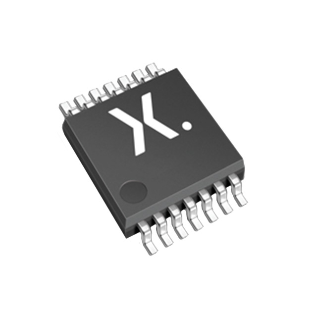
This IC is designed with three inputs and three circuits, providing flexibility in digital logic design. The input logic levels are well-defined, with low levels ranging from 0.12V to 0.8V and high levels from 1.08V to 2V, ensuring compatibility with various digital systems. The 74LVC11PW,118 is packaged in a 14TSSOP format and is available in a tape and reel (TR) package, ideal for surface mount applications.
74LVC11PW,118 Features
- Low Propagation Delay: With a maximum propagation delay of 6.2ns at 3.3V and 50pF, the 74LVC11PW,118 ensures rapid signal processing, making it suitable for high-speed digital circuits.
- Wide Operating Voltage Range: The IC operates within a supply voltage range of 1.2V to 3.6V, offering flexibility and compatibility with various power supply configurations.
- Defined Input Logic Levels: The input logic levels are clearly defined, with low levels from 0.12V to 0.8V and high levels from 1.08V to 2V, ensuring reliable operation in diverse digital systems.
- Surface Mount Compatibility: The 14TSSOP package and surface mount mounting type make the 74LVC11PW,118 ideal for compact and high-density PCB designs.
- Low Quiescent Current: With a maximum quiescent current of 40 µA, the IC is energy-efficient, making it suitable for battery-powered and low-power applications.
- High Output Current Capability: The 74LVC11PW,118 can handle output currents of up to 24mA for both high and low states, ensuring robust performance.
- Compliance and Safety: The IC is REACH unaffected and RoHS3 compliant, ensuring it meets environmental and safety standards.
- Moisture Sensitivity Level: With an MSL of 1 (unlimited), the 74LVC11PW,118 is suitable for storage and handling in various environmental conditions.
74LVC11PW,118 Applications
The 74LVC11PW,118 is ideal for a variety of applications where high-speed, low-power, and reliable digital logic are required. Some specific use cases include:
- Digital Signal Processing: The low propagation delay and high-speed operation make it suitable for applications requiring fast signal processing, such as in digital communication systems.
- Control Systems: The IC can be used in control systems where precise timing and reliable logic operations are critical, such as in industrial automation and robotics.
- Consumer Electronics: The wide operating voltage range and low quiescent current make it ideal for consumer electronics, including smartphones, tablets, and other portable devices.
- Automotive Electronics: The robustness and compliance with environmental standards make the 74LVC11PW,118 suitable for automotive applications, where reliability and safety are paramount.
- Medical Devices: The IC's reliability and compliance with safety standards make it suitable for medical devices, where accurate and timely signal processing is essential.
Conclusion of 74LVC11PW,118
The 74LVC11PW,118 is a versatile and high-performance AND gate logic IC chip that offers significant advantages over similar models. Its low propagation delay, wide operating voltage range, and defined input logic levels make it suitable for a wide range of digital circuit applications. The surface mount compatibility and low quiescent current further enhance its suitability for compact and energy-efficient designs. With its compliance with environmental and safety standards, the 74LVC11PW,118 is an excellent choice for various industries, including consumer electronics, automotive, and medical devices.
FAQ
| Quantity | Unit Price | Ext. Price |
|---|---|---|
| 50+ | $0.19439 | $9.72 |
| 150+ | $0.17368 | $26.05 |
| 500+ | $0.14784 | $73.92 |
| 2500+ | $0.13633 | $340.82 |
| 5000+ | $0.12943 | $647.15 |
Not available to buy online? Want the lower wholesale price? Please Send RFQ to get best price, we will respond immediately


.png?x-oss-process=image/format,webp/resize,h_32)


