

Nexperia
74LVC126ADB,118
Buffers, Drivers, Receivers, Transceivers

Not available to buy online? Want the lower wholesale price? Please Send RFQ to get best price, we will respond immediately


.png?x-oss-process=image/format,webp/resize,p_30)


74LVC126ADB,118 Description
74LVC126ADB,118 Description
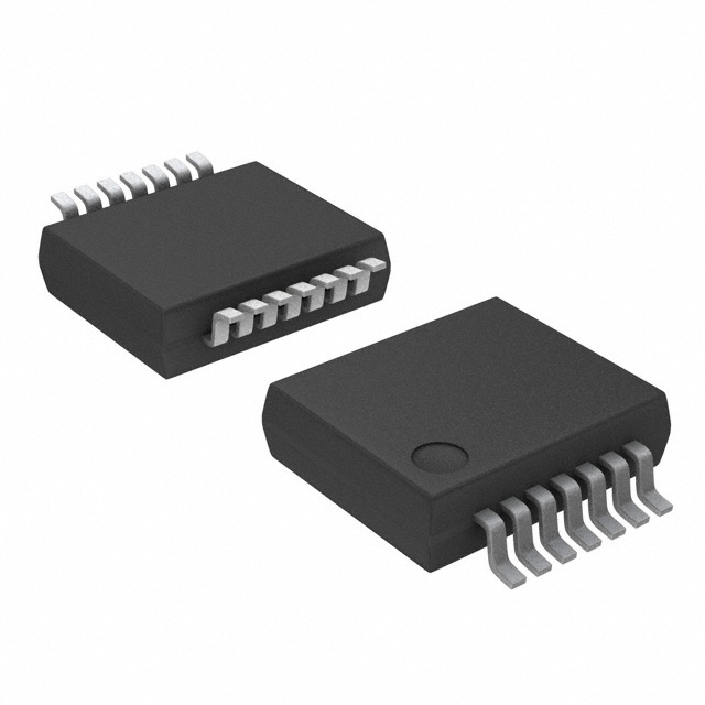
The 74LVC126ADB,118 is a non-inverting buffer IC from Nexperia, designed for high-performance digital signal processing applications. This IC is part of the 74LVC series, known for its low-voltage CMOS technology, which ensures reliable operation across a wide supply voltage range of 1.2V to 3.6V. The device features four independent non-inverting buffers, each capable of handling one bit of data. It is packaged in a 14-pin SSOP (Surface Mount Small Outline Package) and is available in a tape and reel format, making it suitable for automated assembly processes.
74LVC126ADB,118 Features
- Low-Voltage Operation: The 74LVC126ADB,118 operates within a wide supply voltage range of 1.2V to 3.6V, making it compatible with various low-voltage systems and reducing power consumption.
- High Current Capability: Each buffer can source and sink up to 24mA, ensuring robust signal transmission and the ability to drive multiple loads.
- Non-Inverting Buffers: The four non-inverting buffers provide clean and stable output signals, maintaining the integrity of the input data.
- Surface Mount Technology (SMT): The 14SSOP package is ideal for surface mount applications, allowing for compact and reliable integration into modern PCB designs.
- Moisture Sensitivity Level (MSL) 1: The device is classified as MSL 1, meaning it is not moisture-sensitive and can be stored and handled without special precautions.
- Compliance and Safety: The 74LVC126ADB,118 is REACH unaffected and RoHS3 compliant, ensuring it meets environmental and safety standards for electronics manufacturing.
- Obsolete Status: While the product is marked obsolete as, it remains a reliable choice for existing designs and legacy systems where its specific features are required.
74LVC126ADB,118 Applications
The 74LVC126ADB,118 is well-suited for a variety of applications where high-speed signal buffering and low-voltage operation are critical. Some specific use cases include:
- Digital Signal Processing: Ideal for buffering and conditioning digital signals in high-speed communication systems, signal ensuring integrity and reducing noise.
- Embedded Systems: Suitable for use in embedded systems where low power consumption and compact design are essential, such as in IoT devices and microcontrollers.
- Automotive Electronics: The robustness and wide voltage range make it suitable for automotive applications where reliability and performance are paramount.
- Industrial Control Systems: The device can be used in industrial control systems for signal buffering and interfacing between different voltage levels.
- Consumer Electronics: Applicable in consumer for electronics buffering signals in devices such as smartphones, tablets, and other portable electronics.
Conclusion of 74LVC126ADB,118
The 74LVC126ADB,118 offers a reliable and efficient solution for buffering digital signals in a wide range of applications. Its low-voltage operation, high current capability, and robust non-inverting buffers make it a versatile choice for modern electronic designs. Despite its obsolete status, the 74LVC126ADB,118 remains a valuable component for maintaining the functionality of existing systems and ensuring compatibility with low-voltage requirements. Its compliance with environmental and safety standards further enhances its suitability for various industries.
Tech Specifications
74LVC126ADB,118 Documents
Download datasheets and manufacturer documentation for 74LVC126ADB,118
Related Parts


Shopping Guide


.png?x-oss-process=image/format,webp/resize,h_32)


©2025 ERSA Electronics Corporation.