

Nexperia
74LVC139PW,112
Encoders, Decoders, Multiplexers & Demultiplexers

Not available to buy online? Want the lower wholesale price? Please Send RFQ to get best price, we will respond immediately


.png?x-oss-process=image/format,webp/resize,p_30)


74LVC139PW,112 Description
74LVC139PW,112 Description
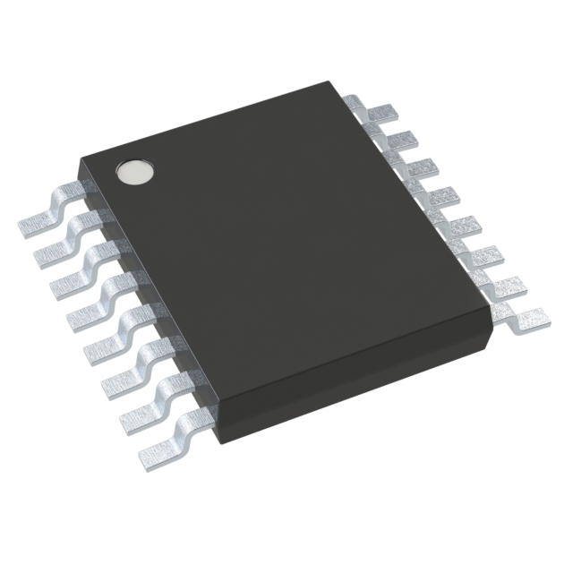
The 74LVC139PW,112 is a high-performance decoder/demultiplexer IC designed for a wide range of digital applications. Manufactured by Nexperia USA Inc., this logic IC chip is part of the 74LVC series and is housed in a 16TSSOP package. It features a 1 x 2:4 decoding circuit, providing two independent circuits for versatile signal routing and control. The device operates on a single supply voltage ranging from 2.7V to 3.6V, making it suitable for low-power applications. With a maximum output current of 24mA for both high and low states, the 74LVC139PW,112 ensures robust performance in various electronic systems.
74LVC139PW,112 Features
- High Performance: The 74LVC139PW,112 offers a wide operating voltage range of 2.7V to 3.6V, ensuring compatibility with a variety of power supply configurations.
- Independent Circuits: It includes two independent 1 x 2:4 decoding circuits, providing enhanced flexibility for complex signal routing and control.
- Surface Mount Technology: The 16TSSOP package supports surface mount technology, enabling efficient and reliable PCB assembly.
- Low Power Consumption: Designed for low power applications, the single supply voltage requirement minimizes energy consumption.
- Compliance and Safety: The device is REACH unaffected and RoHS3 compliant, ensuring environmental and safety standards are met.
- Moisture Sensitivity Level: With an MSL rating of 1 (Unlimited), the 74LVC139PW,112 is suitable for use in a wide range of environmental conditions without the need for special handling.
74LVC139PW,112 Applications
The 74LVC139PW,112 is ideal for applications requiring efficient signal decoding and demultiplexing. Its versatile design makes it suitable for:
- Digital Signal Processing: In systems where multiple signals need to be routed and controlled, the 74LVC139PW,112 provides reliable and efficient decoding.
- Microcontroller Interfaces: Enhances the functionality of microcontrollers by providing additional decoding and demultiplexing capabilities.
- Memory Address Decoding: Ideal for decoding memory addresses in various memory systems, ensuring accurate and efficient data access.
- Communication Systems: Used in communication systems for signal routing and control, improving overall system performance and reliability.
Conclusion of 74LVC139PW,112
The 74LVC139PW,112 is a versatile and reliable decoder/demultiplexer IC that offers significant advantages over similar models. Its wide operating voltage range, independent decoding circuits, and surface mount technology make it an excellent choice for a variety of digital applications. With its compliance to environmental and safety standards, the 74LVC139PW,112 ensures long-term reliability and performance. While the product is now obsolete, its unique features and benefits continue to make it a valuable component in legacy systems and specialized applications.
Tech Specifications
74LVC139PW,112 Documents
Download datasheets and manufacturer documentation for 74LVC139PW,112
ICN6 to ICN8 Transfer 13/Jul/2013 74LVC139 All Dev Label Chgs 2/Aug/2020 Logo 10/Dec/2016 Mult Dev EOL 21/Jul/2021 Mult Dev EOL 5/Jul/2021 74LVC139 Related Parts


Shopping Guide


.png?x-oss-process=image/format,webp/resize,h_32)


©2025 ERSA Electronics Corporation.