
 German
 Japanese
 Portuguese
 Korea
Korea
 Mexico
 Dutch
Dutch


Nexperia
74LVC3G06GN,115

Why Choose Us?
Professional Platform
B2B & B2C purchasingDelivery at full speed
1-2 days deliveryWide variety
Original manufacturers365 days guarantee
Responsible quality
.png)


Tech Specifications
74LVC3G06GN,115 Description
74LVC3G06GN,115 Description
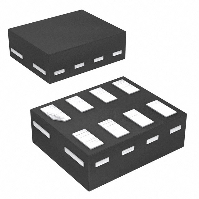
The 74LVC3G06GN,115 is a high-performance, surface-mount logic IC chip designed by Nexperia USA Inc. This device is part of the 74LVC series and functions as a 3-channel inverter with three inputs. It is housed in an 8-pin small outline no-lead (SON) package, which is ideal for compact and high-density PCB designs. The IC operates within a wide supply voltage range of 1.65V to 5.5V, making it suitable for various applications that require flexibility in power supply levels.
One of the key performance metrics of the 74LVC3G06GN,115 is its maximum propagation delay of 2.9ns at 5V and a load capacitance of 50pF. This low propagation delay ensures fast signal processing, which is crucial for high-speed digital circuits. The input logic levels are well-defined, with a low level ranging from 0.7V to 0.8V and a high level from 1.7V to 2V. This precise specification helps in maintaining signal integrity and reducing the risk of signal distortion.
The 74LVC3G06GN,115 also features open-drain outputs, which allow for versatile interfacing with other digital circuits. This feature is particularly useful in applications where multiple devices share a common bus or signal line. The IC is designed to be highly energy-efficient, with a maximum quiescent current of only 4 µA. This low power consumption makes it suitable for battery-operated devices and low-power systems.
74LVC3G06GN,115 Features
- Low Propagation Delay: With a maximum propagation delay of 2.9ns at 5V and 50pF, the 74LVC3G06GN,115 ensures rapid signal processing, making it ideal for high-speed digital applications.
- Wide Supply Voltage Range: The IC operates within a supply voltage range of 1.65V to 5.5V, providing flexibility and compatibility with various power supply levels.
- Open-Drain Outputs: The open-drain feature allows for versatile interfacing with other digital circuits, enabling the use of pull-up resistors and shared signal lines.
- Low Power Consumption: The maximum quiescent current of 4 µA makes the 74LVC3G06GN,115 highly energy-efficient, suitable for low-power and battery-operated devices.
- Surface-Mount Technology: The surface-mount package type ensures ease of integration into modern, high-density PCB designs.
- High Input Logic Levels: Well-defined input logic levels (0.7V to 0.8V for low and 1.7V to 2V for high) ensure signal integrity and reduce the risk of signal distortion.
- Compliance and Safety: The 74LVC3G06GN,115 is REACH unaffected and ROHS3 compliant, ensuring environmental safety and regulatory compliance.
74LVC3G06GN,115 Applications
The 74LVC3G06GN,115 is suitable for a wide range of applications due to its high performance and versatile features. Some specific use cases include:
- High-Speed Digital Systems: The low propagation delay and high-speed performance make it ideal for applications requiring rapid signal processing, such as high-speed data transmission and communication systems.
- Battery-Operated Devices: The low power consumption and wide supply voltage range make it suitable for portable and battery-operated devices, ensuring long battery life and reliable operation.
- Shared Signal Lines: The open-drain outputs allow for easy interfacing with shared signal lines, making it ideal for applications involving multiple devices on a common bus, such as I2C and SPI communication protocols.
- Compact PCB Designs: The surface-mount package type and small form factor make it suitable for high-density PCB designs, where space is a critical constraint.
- Signal Inversion: As an inverter, the 74LVC3G06GN,115 is ideal for applications requiring signal inversion, such as digital logic circuits and control systems.
Conclusion of 74LVC3G06GN,115
The 74LVC3G06GN,115 is a versatile and high-performance logic IC chip that offers a combination of speed, efficiency, and flexibility. Its low propagation delay, wide supply voltage range, and open-drain outputs make it suitable for a wide range of applications, from high-speed digital systems to battery-operated devices. The device's compliance with environmental and safety standards ensures that it meets the requirements of modern electronics manufacturing. Overall, the 74LVC3G06GN,115 is an excellent choice for designers looking for a reliable and efficient inverter solution in their digital circuits.
FAQ
| Quantity | Unit Price | Ext. Price |
|---|---|---|
| 435+ | $0.60720 | $264.13 |
Not available to buy online? Want the lower wholesale price? Please Send RFQ to get best price, we will respond immediately


.png?x-oss-process=image/format,webp/resize,h_32)


