
 German
 Japanese
 Portuguese
 Korea
Korea
 Mexico
 Dutch
Dutch


Nexperia
74LVC574ADB,112

Why Choose Us?
Professional Platform
B2B & B2C purchasingDelivery at full speed
1-2 days deliveryWide variety
Original manufacturers365 days guarantee
Responsible quality
.png)


Tech Specifications
74LVC574ADB,112 Description
74LVC574ADB,112 Description
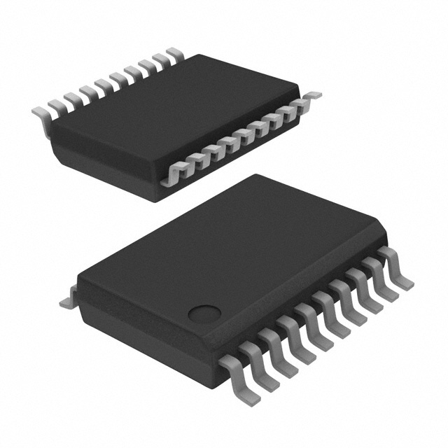
The 74LVC574ADB,112 is a single 8-bit D-type flip-flop integrated circuit (IC) designed for high-performance digital applications. Manufactured by Nexperia USA Inc., this IC is part of the 74LVC series, known for its robustness and versatility in various electronic systems. The device operates within a wide supply voltage range of 1.65V to 3.6V, making it suitable for a variety of power supply conditions. It features a clock frequency of up to 200 MHz, ensuring high-speed operation and efficient data handling.
74LVC57ADB4,112 Features
- Clock Frequency: The 74LVC574ADB,112 supports a clock frequency of up to 200 MHz, enabling rapid data processing and synchronization.
- Trigger Type: It employs a positive edge-trigger mechanism, ensuring reliable and precise data capture.
- Supply Voltage: The IC operates within a supply voltage range of 1.65V to 3.6V, providing flexibility in power supply design.
- Max Propagation Delay: With a maximum propagation delay of 7ns at 3.3V and 50pF, the device ensures minimal latency in signal transmission.
- Low Quiescent Current: The IC consumes only 10 µA in quiescent mode, contributing to energy efficiency.
- Output Current Capability: It can drive both high and low outputs with a current of 24mA, ensuring robust signal integrity.
- Input Capacitance: The low input capacitance of 5 pF minimizes loading effects on the driving circuit.
- Compliance and Standards: The 74LVC574ADB,112 is REACH unaffected and RoHS3 compliant, meeting stringent environmental and safety standards.
- Moisture Sensitivity Level: With an MSL of 1 (Unlimited), the IC is suitable for extended storage and handling without moisture-related degradation.
74LVC574ADB,112 Applications
The 74LVC574ADB,112 is ideal for a range of applications requiring high-speed, reliable data storage and processing. Its features make it particularly suitable for:
- Digital Systems: Use in digital signal processing, microcontroller interfacing, and data communication systems.
- Memory Applications: Ideal for temporary data storage and buffering in memory modules and data processing units.
- High-Speed Data Handling: Suitable for applications requiring rapid data capture and synchronization, such as high in-speed counters and shift registers.
- Industrial Control Systems: Employed in control systems where reliable data storage and processing are critical.
Conclusion of 74LVC574ADB,112
The 74LVC574ADB,112 is a versatile and high-performance D-type flip-flop IC, offering a combination of speed, efficiency, and reliability. Its wide supply voltage range, low quiescent current, and robust output current capability make it for suitable a variety of digital applications. Despite being marked as obsolete, the 74LVC574ADB,112 remains a reliable choice for engineers and designers seeking a proven solution for their digital circuitry needs.
FAQ
Not available to buy online? Want the lower wholesale price? Please Send RFQ to get best price, we will respond immediately


.png?x-oss-process=image/format,webp/resize,h_32)


