

Nexperia
XS3A4053PWJ
Analog Switches, Multiplexers, Demultiplexers

Not available to buy online? Want the lower wholesale price? Please Send RFQ to get best price, we will respond immediately


.png?x-oss-process=image/format,webp/resize,p_30)


XS3A4053PWJ Description
XS3A4053PWJ Description
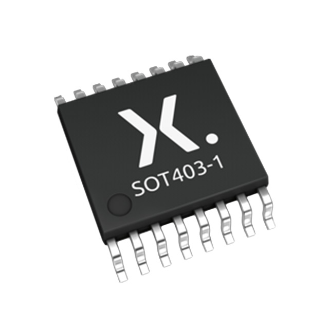
The XS3A4053PWJ is a high-performance, single-pole double-throw (SPDT) switch IC designed for demanding applications requiring reliable signal routing. Manufactured by Nexperia USA Inc., this interface IC chip is housed in a 16-lead TSSOP package, ensuring robustness and ease of integration into various electronic systems. The device operates within a wide supply voltage range of 1.4V to 4.3V, making it suitable for a variety of power supply configurations.
XS3A4053PWJ Features
- Low Leakage Current: With a maximum leakage current of only 10nA, the XS3A4053PWJ ensures minimal power consumption and high signal integrity, even in low-power applications.
- Channel-to-Channel Matching: The device offers excellent channel-to-channel matching with a maximum ΔRon of 130mOhm, ensuring consistent performance across multiple channels.
- Low On-State Resistance: The maximum on-state resistance of 900mOhm minimizes power loss and ensures efficient signal transmission.
- High Bandwidth: The -3dB bandwidth of 40MHz supports high-frequency signal routing, making it ideal for applications requiring fast data transfer.
- Fast Switching Times: The XS3A4053PWJ boasts switch times of 20ns for turn-on and 40ns for turn-off, enabling rapid signal switching without compromising signal quality.
- Low Charge Injection: With a charge injection of only 15pC, the device minimizes signal distortion during switching, ensuring clean signal transmission.
- Compliance and Reliability: The XS3A4053PWJ is REACH unaffected and RoHS3 compliant, adhering to stringent environmental and safety standards. It also has a moisture sensitivity level (MSL) of 1, indicating unlimited shelf life, which enhances its reliability in various environmental conditions.
- Multiplexer/Demultiplexer Circuit: The 2:1 multiplexer/demultiplexer circuit allows for efficient signal routing and switching, making it versatile for complex signal management tasks.
XS3A4053PWJ Applications
The XS3A4053PWJ is well-suited for a variety of applications where signal integrity and efficient switching are critical. Some specific use cases include:
- Telecommunications: Ideal for routing and switching high-frequency signals in communication systems, ensuring minimal signal degradation and fast data transfer.
- Data Acquisition Systems: Its low on-state resistance and high bandwidth make it suitable for applications requiring precise signal acquisition and processing.
- Automotive Electronics: The device's robustness and compliance with environmental standards make it a reliable choice for automotive applications, where reliability and performance are paramount.
- Industrial Control Systems: The XS3A4053PWJ can be used in industrial control systems for signal routing and switching, ensuring efficient operation and minimal downtime.
- Consumer Electronics: Its compact size and high performance make it suitable for consumer electronics, where space and efficiency are critical factors.
Conclusion of XS3A4053PWJ
The XS3A4053PWJ is a versatile and high-performance SPDT switch IC that offers significant advantages over similar models. Its low leakage current, excellent channel-to-channel matching, and low on-state resistance ensure minimal power loss and high signal integrity. The device's fast switching times and high bandwidth make it suitable for a wide range of applications, from telecommunications to consumer electronics. With its compliance with environmental and safety standards, the XS3A4053PWJ is a reliable and efficient choice for modern electronic systems.
Tech Specifications
XS3A4053PWJ Documents
Download datasheets and manufacturer documentation for XS3A4053PWJ
XS3A4053 Related Parts


Shopping Guide


.png?x-oss-process=image/format,webp/resize,h_32)


©2025 ERSA Electronics Corporation.