
 German
 Japanese
 Portuguese
 Korea
Korea
 Mexico
 Dutch
Dutch



NXP Semiconductors
74HC3G04DC,125


Why Choose Us?
Professional Platform
B2B & B2C purchasingDelivery at full speed
1-2 days deliveryWide variety
Original manufacturers365 days guarantee
Responsible quality

.png)


Tech Specifications
74HC3G04DC,125 Description
74HC3G04DC,125 Description
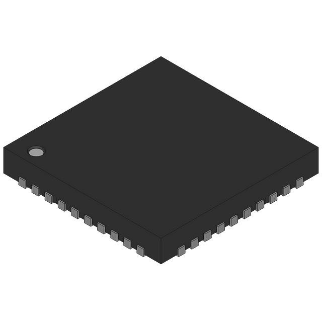
The 74HC3G04DC,125 is a high-performance logic IC chip designed by NXP Semiconductors, a leading manufacturer in the semiconductor industry. This device is part of the 74HC series and functions as a triple inverter with three independent inputs and outputs. It is packaged in an 8VSSOP format, making it suitable for surface-mount applications. The 74HC3G04DC,125 operates within a supply voltage range of 2V to 6V, offering flexibility in various power supply configurations. It is designed to handle a maximum propagation delay of 13 nanoseconds at 6V with a load capacitance of 50 picofarads, ensuring fast and reliable signal inversion.
74HC3G04DC,125 Features
- Triple Inverter Functionality: The 74HC3G04DC,125 features three independent inverter circuits, each capable of inverting the input signal. This allows for efficient handling of multiple signals within a single compact package.
- Wide Operating Voltage Range: With a supply voltage range of 2V to 6V, the 74HC3G04DC,125 can be used in a variety of systems with different power supply requirements.
- Low Quiescent Current: The device consumes a maximum of 1 µA in quiescent state, making it highly energy-efficient and suitable for low-power applications.
- High Output Current Capability: The 74HC3G04DC,125 can source and sink up to 5.2mA, ensuring robust performance and compatibility with a wide range of load conditions.
- Fast Propagation Delay: At a maximum of 13ns with a 50pF load at 6V, the 74HC3G04DC,125 ensures rapid signal processing, which is crucial for high-speed digital circuits.
- Surface-Mount Technology (SMT): The 8VSSOP package format is ideal for surface-mount applications, providing ease of integration into modern PCB designs.
- Input Logic Levels: The device supports input logic levels of 0.5V to 1.8V for low and 1.5V to 4.2V for high, ensuring compatibility with a wide range of digital systems.
74HC3G04DC,125 Applications
The 74HC3G04DC,125 is ideal for a variety of applications where signal inversion is required. Its triple inverter functionality and compact size make it suitable for:
- Digital Signal Processing: Inverting signals in digital circuits to achieve the desired logic state.
- Clock Signal Generation: Generating inverted clock signals for synchronous digital systems.
- Data Transmission: Inverting data signals in communication systems to ensure proper signal integrity.
- Control Systems: Inverting control signals in microcontroller-based systems to manage various functions.
- Consumer Electronics: Used in devices where compact and efficient signal inversion is necessary, such as in smartphones, tablets, and other portable electronics.
Conclusion of 74HC3G04DC,125
The 74HC3G04DC,125 is a versatile and high-performance logic IC chip that offers significant advantages over similar models. Its triple inverter functionality, wide operating voltage range, and low quiescent current make it an excellent choice for a variety of applications. The fast propagation delay and high output current capability ensure reliable and efficient signal inversion, making it suitable for high-speed digital circuits. The surface-mount package format further enhances its ease of integration into modern PCB designs. Overall, the 74HC3G04DC,125 is a reliable and efficient solution for digital signal inversion needs in the electronics industry.
FAQ
Not available to buy online? Want the lower wholesale price? Please Send RFQ to get best price, we will respond immediately






.png?x-oss-process=image/format,webp/resize,h_32)


