NXP Semiconductors
LPC11A12FHN33/101,
Microcontrollers


.png?x-oss-process=image/format,webp/resize,p_30)


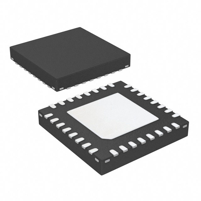
LPC11A12FHN33/101, Description
The LPC11A12FHN33/101 is a low-power microcontroller (MCU) from NXP Semiconductors, specifically designed for applications requiring low power consumption and high performance. It is based on the 32-bit ARM Cortex-M0+ processor and is part of the LPC11A12 family of MCUs.
Description:
The LPC11A12FHN33/101 is a high-performance, low-power MCU that features a 32-bit ARM Cortex-M0+ processor with a clock speed of up to 50 MHz. It is equipped with 64 Kbytes of on-chip flash memory and 20 Kbytes of SRAM. The MCU also includes a range of communication interfaces, including I2C, SPI, and UART, as well as a USB interface for easy connectivity.
Features:
- 32-bit ARM Cortex-M0+ processor with clock speeds up to 50 MHz
- 64 Kbytes of on-chip flash memory
- 20 Kbytes of SRAM
- Low power consumption with multiple power-saving modes
- USB 2.0 full-speed interface
- I2C, SPI, and UART communication interfaces
- 10-bit ADC with up to 8 channels
- Flexible clocking options with an internal RC oscillator or external clock sources
- Support for GPIO and various peripheral interfaces
- Small package options available for space-constrained applications
Applications:
The LPC11A12FHN33/101 is suitable for a wide range of applications that require low power consumption and high performance. Some potential applications include:
- Battery-powered devices, such as wearables, portable medical devices, and remote sensors
- Industrial control and monitoring systems
- Home automation and smart home devices
- IoT devices and edge nodes
- Wireless communication modules, such as Zigbee or BLE nodes
- Automotive control systems, such as window control or tire pressure monitoring
- Consumer electronics, such as portable media players and gaming accessories
- Medical equipment, such as portable monitoring devices and diagnostic tools
The LPC11A12FHN33/101's low power consumption, high performance, and versatile feature set make it an ideal choice for a wide range of embedded applications that require efficient and reliable processing capabilities.
Tech Specifications
LPC11A12FHN33/101, Documents
Download datasheets and manufacturer documentation for LPC11A12FHN33/101,
 LPC11Axx
  All Dev Label Update 15/Dec/2020 Mult Dev Pkg Seal 15/Dec/2020
  LPC11Axx
  NXP USA Inc REACH NXP USA Inc RoHS Cert
 Shopping Guide


.png?x-oss-process=image/format,webp/resize,h_32)


