NXP Semiconductors
LPC11E12FBD48/201,
Microcontrollers


.png?x-oss-process=image/format,webp/resize,p_30)


LPC11E12FBD48/201, Description
The LPC11E12FBD48/201 is a low-power microcontroller (MCU) from NXP Semiconductors, specifically designed for applications that require low power consumption and high performance. Here's a brief description, features, and applications of the LPC11E12FBD48/201:
Description:
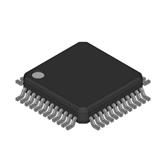
The LPC11E12FBD48/201 is a member of the LPC1100 series, which is based on the 32-bit ARM Cortex-M0+ processor. It operates at a maximum frequency of 12 MHz and is fabricated using a 180nm CMOS process. The device is available in a 48-pin LQFP (Low Profile Quad Flat Package) package.
Features:
- ARM Cortex-M0+ processor with a maximum frequency of 12 MHz.
- 64KB on-chip Flash memory and 8KB on-chip RAM.
- 8-channel 10-bit ADC (Analog-to-Digital Converter) with up to 1Msps (million samples per second) conversion rate.
- 2-channel DAC (Digital-to-Analog Converter) with 10-bit resolution.
- USB 2.0 full-speed device interface with integrated PHY.
- UART (Universal Asynchronous Receiver-Transmitter) interface for serial communication.
- SPI (Serial Peripheral Interface) and I2C (Inter-Integrated Circuit) interfaces for communication with external devices.
- 4-channel DMA (Direct Memory Access) controller for efficient data transfer.
- Flexible clock management system with an internal RC oscillator, an external clock input, and a low-power RTC (Real-Time Clock) oscillator.
- Power management features, including a low-power sleep mode and power scaling to optimize power consumption.
- Up to 18 GPIO (General-Purpose Input/Output) pins with various functions and configurable pull-ups.
- CRC (Cyclic Redundancy Check) engine for error detection.
- Nested Vectored Interrupt Controller (NVIC) for efficient interrupt handling.
- Support for JTAG (Joint Test Action Group) and SWD (Serial Wire Debug) interfaces for debugging and testing.
Applications:
The LPC11E12FBD48/201 is suitable for a wide range of applications that require low power consumption and high performance. Some typical applications include:
- Battery-powered devices, such as portable medical equipment, fitness trackers, and smart watches.
- Industrial control and monitoring systems, including sensor interfaces and data acquisition.
- Smart home and IoT (Internet of Things) devices, including smart lighting, thermostats, and home automation systems.
- Automotive applications, such as infotainment systems, body control modules, and sensor interfaces.
- Wearable electronics, including smart glasses, smartwatches, and fitness bands.
- Consumer electronics, such as portable media players, e-book readers, and wireless speakers.
- Embedded systems in various industries, including healthcare, security, and telecommunications.
The LPC11E12FBD48/201's low-power capabilities, integrated peripherals, and ease of use make it an attractive choice for developers looking to create energy-efficient and high-performance embedded systems.
Tech Specifications
LPC11E12FBD48/201, Documents
Download datasheets and manufacturer documentation for LPC11E12FBD48/201,
Shopping Guide


.png?x-oss-process=image/format,webp/resize,h_32)


