

NXP Semiconductors
LPC2104BBD48,151
Microcontrollers

Not available to buy online? Want the lower wholesale price? Please Send RFQ to get best price, we will respond immediately


.png?x-oss-process=image/format,webp/resize,p_30)


LPC2104BBD48,151 Description
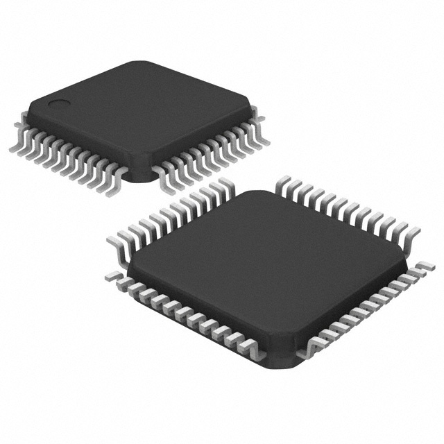
The LPC2104BBD48,151 is a microcontroller unit (MCU) developed by NXP Semiconductors. It is part of the LPC2104 family of MCUs, which are based on the ARM7TDMI-S processor core. The "BBD48,151" in the model number refers to the package type and memory configuration of the device.
Description:
The LPC2104BBD48,151 is a high-performance, low-power, 32-bit MCU designed for a wide range of embedded applications. It features an ARM7TDMI-S processor core, which is optimized for real-time performance and low power consumption. The device is housed in a 48-pin LQFP (Low Profile Quad Flat Package) package.
Features:
- ARM7TDMI-S processor core with a clock speed of up to 60 MHz.
- 512KB on-chip flash memory for program storage.
- 64KB on-chip static RAM (SRAM) for data storage.
- Advanced memory protection unit (MPU) for enhanced security.
- Integrated peripheral set, including UART, SPI, I2C, and USB interfaces.
- Flexible clocking options, including an internal RC oscillator, external crystal, or clock input.
- Power management features, such as sleep and deep sleep modes, to reduce power consumption.
- 48 general-purpose I/O pins with various functions and support for multiplexed I/O.
- On-chip debugging and trace capabilities, compatible with JTAG and SWD (Serial Wire Debug) interfaces.
- Operating temperature range of -40°C to +85°C.
Applications:
The LPC2104BBD48,151 is suitable for a wide range of embedded applications, including but not limited to:
- Industrial control and automation systems.
- Medical devices and equipment.
- Consumer electronics, such as portable devices and smart appliances.
- Automotive applications, such as infotainment systems and body control modules.
- Networking and communication devices, including routers, modems, and IoT devices.
- Data acquisition and signal processing systems.
- Embedded systems requiring real-time performance and low power consumption.
The LPC2104BBD48,151's combination of processing power, memory, and peripheral integration makes it a versatile choice for developers looking to create efficient and reliable embedded systems.
Tech Specifications
LPC2104BBD48,151 Documents
Download datasheets and manufacturer documentation for LPC2104BBD48,151
LPC2104-06 All Dev Label Update 15/Dec/2020 LPC2104-06 NXP USA Inc REACH NXP USA Inc RoHS Cert Related Parts


Shopping Guide


.png?x-oss-process=image/format,webp/resize,h_32)


©2025 ERSA Electronics Corporation.