

NXP Semiconductors
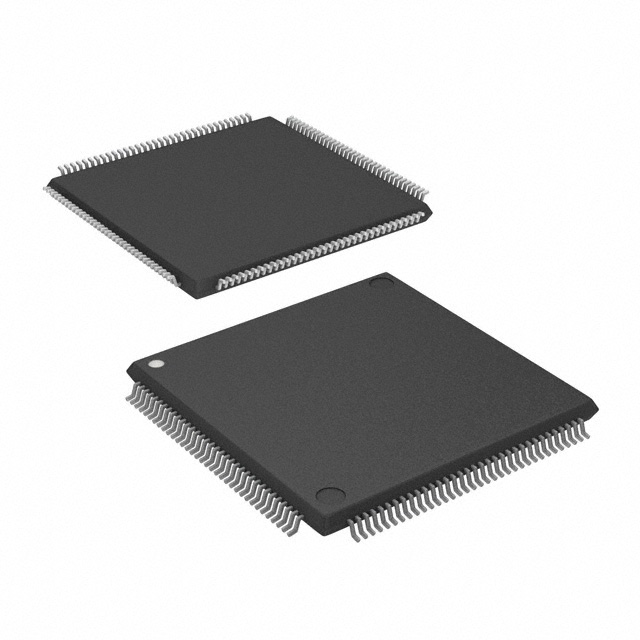
LPC4088FBD144,551
Microcontrollers

Not available to buy online? Want the lower wholesale price? Please Send RFQ to get best price, we will respond immediately


.png?x-oss-process=image/format,webp/resize,p_30)


LPC4088FBD144,551 Description
The LPC4088FBD144,551 is a high-performance microcontroller unit (MCU) from NXP Semiconductors. It belongs to the LPC4000 family of MCUs, which are designed for a wide range of applications, including industrial control, medical equipment, consumer electronics, and automotive systems.
Description:
The LPC4088FBD144,551 is a 144-pin, fine pitch ball grid array (FBGA) package. It features an ARM Cortex-M4 CPU with a 2048 KB on-chip SRAM, which provides high performance and efficient power consumption. The device also includes a range of integrated peripherals, including USB, Ethernet, and various communication interfaces, making it suitable for a wide range of applications.
Features:
- ARM Cortex-M4 CPU with 1.25 DMIPS/MHz performance and a floating-point unit (FPU)
- 2048 KB on-chip SRAM
- 144-pin fine pitch ball grid array (FBGA) package
- USB high-speed device/host/OTG controller
- 10/100 Ethernet MAC with PHY
- Advanced control and debug features
- Integrated SRAM and EEPROM emulation
- Multiple communication interfaces, including UART, SPI, I2C, CAN, and LIN
- Advanced analog peripherals, including 12-bit ADC, comparators, and operational amplifiers
- Flexible power management with low-power sleep modes
Applications:
The LPC4088FBD144,551 is suitable for a wide range of applications, including:
- Industrial control systems
- Medical equipment
- Consumer electronics, such as smart home devices and portable gadgets
- Automotive systems, including infotainment and body control modules
- Networking and communication devices, such as routers and gateways
- Human-machine interface (HMI) devices
- IoT devices and edge computing applications
- Audio and video processing systems
- Data acquisition and signal processing applications
The LPC4088FBD144,551's combination of high performance, advanced peripherals, and flexible power management makes it an excellent choice for a wide range of embedded systems requiring high processing capabilities and efficient power consumption.
Tech Specifications
LPC4088FBD144,551 Documents
Download datasheets and manufacturer documentation for LPC4088FBD144,551
LPC407x/8x Leaflet LPC408x/7x All Dev Label Update 15/Dec/2020 Mult Dev Pkg Seal 15/Dec/2020 LPC407x/8x Block Diagram LPC407x/8x Leaflet LPC407x/408x Datasheet Update 05/Jun/2014 NXP USA Inc REACH NXP USA Inc RoHS Cert Related Parts


Shopping Guide


.png?x-oss-process=image/format,webp/resize,h_32)


©2025 ERSA Electronics Corporation.