NXP Semiconductors_NX5DV330PW,112

NXP Semiconductors
NX5DV330PW,112  
Analog Switches - Special Purpose ICs

NXP Semiconductors
NX5DV330PW,112
780-NX5DV330PW,112
Ersa
NXP Semiconductors-NX5DV330PW,112-datasheets-7216751.pdf
IC VIDEO MUX/DEMUX 1X2 16TSSOP
In Stock : 2323

Not available to buy online? Want the lower wholesale price? Please Send RFQ to get best price, we will respond immediately

QUICK RFQ
ADD TO RFQ LIST
ersa FreeSample ersa flow
ISO9001
Quality Policy
ISO45001
ISO14001

NX5DV330PW,112 Description

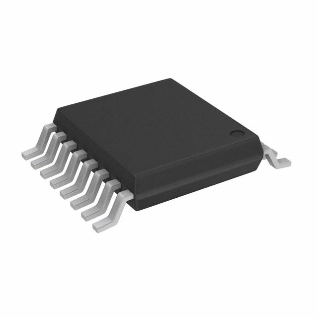
The Tube for this electronic equipment is available. The packaging way of this NX5DV330PW,112 is to conserve time, space, energy, and resources. This NX5DV330PW,112 offers cheap cost, adaptability, dependability, efficiency, and consistency. This NX5DV330PW,112 is produced by NXP Semiconductors and is used in a variety of industries. This manufacturer aspires to rank among the top electronic vendors in the Asia-Pacific region. Additionally, it hopes to contribute significantly to the sector's expansion. This NX5DV330PW,112 falls under the Analog Switches - Special Purpose ICs category. The most advanced level of this category is Interface IC Chips. IC interfaces differ in terms of device types and applications. Some products are used with buffers, cardbus controllers, and crosspoint switches.

Tech Specifications

Operating Temperature
Applications
ECCN
-3db Bandwidth
Mounting Type
Product Status
Supplier Device Package
Voltage - Supply, Dual (V±)
Voltage - Supply, Single (V+)
Series
Package / Case
Number of Channels
On-State Resistance (Max)
Switch Circuit
REACH Status
Mfr
Features
Multiplexer/Demultiplexer Circuit
HTSUS
Package
RoHS Status
Base Product Number
Moisture Sensitivity Level (MSL)
Number of Channels per Chip
Power Supply Type
Output Signal Type
Configuration
PCB changed
ECCN (US)
PPAP
Maximum Turn-On Time (ns)
Maximum Power Dissipation (mW)
Automotive
Minimum Operating Temperature (°C)
Maximum Operating Temperature (°C)
Supplier Package
Package Height
EU RoHS
Maximum On Resistance (Ohm)
Maximum Turn-Off Time (ns)
Typical Single Supply Voltage (V)
Number of Inputs per Chip
Maximum Frequency (25°C) @ Vcc (MHz)
Number of Outputs per Chip
Chip Enable Signals
Package Length
Standard Package Name
Maximum On Resistance Range (Ohm)
Pin Count
Mounting
Type
Input Signal Type
Maximum Single Supply Voltage (V)
Minimum Single Supply Voltage (V)
Lead Shape
Part Status
Package Width
Multiplexer Architecture

NX5DV330PW,112 Documents

Download datasheets and manufacturer documentation for NX5DV330PW,112

Ersa PM72 process transfer 24/Jul/2013      
Ersa NX5DV330      
Ersa All Dev Label Update 15/Dec/2020      
Ersa Multiple Devices 05/Jul/2015      
Ersa NX5DV330      
Ersa NXP USA Inc REACH       NXP USA Inc RoHS Cert      

Shopping Guide

Payment Methods
Payment Methods include Prepayment TT (bank transfer), Western Union, and PayPal. Customers are responsible for shipping costs, bank charges, customs duties and taxes.
Shipping Rate
Shipments are made once a day around 5pm, excluding Sundays. Once shipped, the estimated delivery time is usually 5-7 business days, depending on the courier you choose.
Delivery Methods
Provide DHL, FedEx, UPS, EMS, SF Express and Registered Airmail International Delivery Service