
 German
 Japanese
 Portuguese
 Korea
Korea
 Mexico
 Dutch
Dutch


onsemi
4N33VM
903-4N33VM

PDF Datasheet
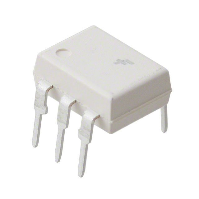
6-Pin DIP General Purpose Photodarlington Optocoupler, 1000-BLKBG
10 Weeks
Why Choose Us?
Professional Platform
B2B & B2C purchasingDelivery at full speed
1-2 days deliveryWide variety
Original manufacturers365 days guarantee
Responsible quality
.png)


Tech Specifications
Package/Case
DIP
Collector Emitter Saturation Voltage
1V
Collector Emitter Voltage (VCEO)
1V
Collector-emitter Voltage-Max
1V
Contact Plating
Tin, Matte
Input Type
DC
Isolation Voltage-Max
5.3kV
Lead Free
Lead Free
4N33VM Description
Optoisolator Darlington with Base Output 4170Vrms 1 Channel 6-DIP
FAQ
What is the standard lead time for 4N33VM?
The standard lead time for 4N33VM is 10 Weeks.
What package or case is 4N33VM available in?
What voltage specification is listed for 4N33VM?
What operating temperature range does 4N33VM support?
Is 4N33VM currently in stock?
Quick Quote
ADD TO RFQ LIST
Not available to buy online? Want the lower wholesale price? Please Send RFQ to get best price, we will respond immediately
QUICK RFQ


.png?x-oss-process=image/format,webp/resize,h_32)


