
 German
 Japanese
 Portuguese
 Korea
Korea
 Mexico
 Dutch
Dutch


Why Choose Us?
Professional Platform
B2B & B2C purchasingDelivery at full speed
1-2 days deliveryWide variety
Original manufacturers365 days guarantee
Responsible quality
.png)


Tech Specifications
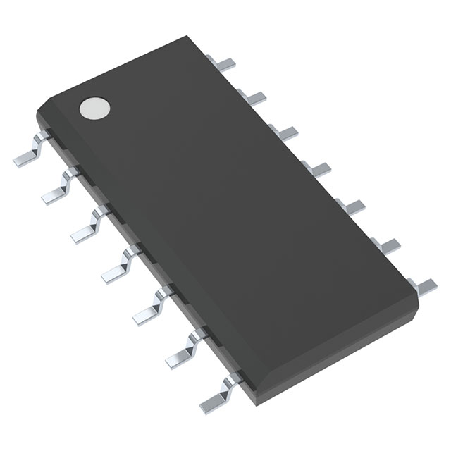
74HC74DR2G Description
74HC74DR2G Description
The 74HC74DR2G is a dual D-type flip-flop IC, designed for high-speed digital applications. Manufactured by onsemi, this device is part of the 74HC series, known for its robust performance and reliability. The 74HC74DR2G features a clock frequency of up to 28 MHz, making it suitable for demanding digital circuits. It operates within a supply voltage range of 2V to 6V, providing flexibility in power supply requirements. The IC offers complementary outputs, ensuring versatile connectivity and signal integrity. With a positive edge trigger type, it ensures precise timing control, crucial for synchronous operations in digital systems.
74HC74DR2G Features
- High-Speed Operation: The 74HC74DR2G supports a clock frequency of up to 28 MHz, enabling it to handle high-speed digital signals efficiently.
- Complementary Outputs: This feature allows for both true and complement outputs, enhancing the flexibility of the IC in various digital circuits.
- Positive Edge Triggering: Ensures that the flip-flop captures data on the rising edge of the clock signal, providing precise timing control.
- Low Quiescent Current: With a quiescent current of only 2 µA, the 74HC74DR2G is energy-efficient, making it suitable for low-power applications.
- Wide Supply Voltage Range: The device operates within a supply voltage range of 2V to 6V, offering flexibility in power supply requirements.
- Low Propagation Delay: A maximum propagation delay of 17 ns at 6V and 50 pF ensures fast signal transmission, crucial for high-speed applications.
- Surface Mount Packaging: The 74HC74DR2G is available in a surface mount package, facilitating easy integration into modern PCB designs.
- Moisture Sensitivity Level 1: The device is classified as MSL 1, indicating it is not sensitive to moisture, making it suitable for a wide range of environmental conditions.
- REACH Compliance: The 74HC74DR2G is REACH unaffected, ensuring compliance with environmental and health regulations.
74HC74DR2G Applications
The 74HC74DR2G is ideal for a variety of applications due to its high-speed operation, low power consumption, and versatile output capabilities. Some specific use cases include:
- Digital Clock Circuits: The positive edge triggering and high clock frequency make it suitable for generating precise clock signals in digital systems.
- Data Latching: The dual D-type flip-flops can be used to latch data in synchronous digital circuits, ensuring data integrity during transmission.
- Frequency Dividers: The device can be configured to divide input frequencies, useful in applications requiring lower frequency outputs.
- Edge Detection Circuits: The positive edge triggering feature allows the 74HC74DR2G to be used in edge detection circuits, capturing and processing signal transitions accurately.
- Memory Elements: The flip-flops can serve as memory elements in digital circuits, storing single bits of data.
Conclusion of 74HC74DR2G
The 74HC74DR2G is a versatile dual D-type flip-flop IC, offering high-speed operation, low power consumption, and complementary outputs. Its positive edge triggering and wide supply voltage range make it suitable for a variety of digital applications. Despite being marked as obsolete, the 74HC74DR2G remains a reliable choice for engineers and designers looking for a robust and efficient flip-flop solution. Its compliance with REACH regulations and moisture sensitivity level 1 classification further enhance its suitability for diverse environments. For applications requiring precise timing control and high-speed data processing, the 74HC74DR2G is an excellent choice.
FAQ
Not available to buy online? Want the lower wholesale price? Please Send RFQ to get best price, we will respond immediately


.png?x-oss-process=image/format,webp/resize,h_32)


