
 German
 Japanese
 Portuguese
 Korea
Korea
 Mexico
 Dutch
Dutch


Why Choose Us?
Professional Platform
B2B & B2C purchasingDelivery at full speed
1-2 days deliveryWide variety
Original manufacturers365 days guarantee
Responsible quality
.png)


Tech Specifications
AU5517DR2G Description
AU5517DR2G Description
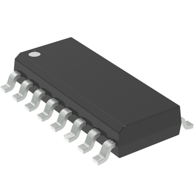
The AU5517DR2G is a high-performance transconductance operational amplifier designed by onsemi, featuring two circuits in a 16-SOIC package. This IC is optimized for demanding applications requiring high slew rates and low input bias current. With a maximum supply voltage span of 44V and a gain bandwidth product of 2 MHz, the AU5517DR2G offers robust performance in a compact surface-mount package. The amplifier is designed to operate at an extended temperature range up to 150°C (TJ), making it suitable for high-temperature environments. The device also features a low input bias current of 400 nA and a supply current of 2.6mA, ensuring efficient power consumption. The AU5517DR2G is REACH unaffected and RoHS3 compliant, adhering to stringent environmental regulations. The moisture sensitivity level (MSL) of 1 (Unlimited) ensures the device remains stable under various environmental conditions.
AU5517DR2G Features
- High Slew Rate: The AU5517DR2G boasts a high slew rate of 50V/µs, enabling it to handle fast signal transitions with minimal distortion.
- Low Input Bias Current: With an input bias current of only 400 nA, the AU5517DR2G minimizes the impact of input currents on the signal, ensuring high accuracy and stability.
- Wide Supply Voltage Range: The device operates within a supply voltage range of 44V, providing flexibility in power supply design.
- High Operating Temperature: The AU5517DR2G is rated for operation up to 150°C (TJ), making it ideal for high-temperature industrial and automotive applications.
- Low Input Offset Voltage: The low input offset voltage of 400 µV ensures precise signal amplification and reduces errors in signal processing.
- Dual Circuit Design: The dual circuit design allows for multiple amplification stages or parallel processing in a single package, optimizing space and reducing component count.
- Environmental Compliance: The AU5517DR2G is REACH unaffected and RoHS3 compliant, ensuring it meets the latest environmental standards without compromising performance.
- Moisture Sensitivity Level: The MSL of 1 (Unlimited) ensures the device remains stable and reliable in various environmental conditions, reducing the risk of moisture-related failures.
AU5517DR2G Applications
The AU5517DR2G is well-suited for a variety of applications where high performance and reliability are critical. Its high slew rate and low input bias current make it ideal for applications requiring fast and accurate signal processing. Some specific use cases include:
- Industrial Control Systems: The high operating temperature and robust performance make the AU5517DR2G suitable for industrial control systems where precision and reliability are paramount.
- Automotive Electronics: The extended temperature range and moisture sensitivity level ensure the device remains stable in the demanding environments typical of automotive applications.
- Signal Processing: The low input bias current and high slew rate make the AU5517DR2G ideal for signal processing applications where fast and accurate amplification is required.
- Telecommunications: The device's high performance and environmental compliance make it suitable for telecommunications equipment where reliability and precision are essential.
Conclusion of AU5517DR2G
The AU5517DR2G is a versatile and high-performance transconductance operational amplifier designed to meet the demands of modern electronics applications. Its high slew rate, low input bias current, and wide supply voltage range provide exceptional performance, while its environmental compliance and robustness ensure reliability in various conditions. Although the product is now obsolete, it remains a testament to onsemi's commitment to delivering high-quality and innovative solutions for the electronics industry. For applications requiring high performance and reliability, the AU5517DR2G remains a viable option, offering significant advantages over similar models.
FAQ
Not available to buy online? Want the lower wholesale price? Please Send RFQ to get best price, we will respond immediately


.png?x-oss-process=image/format,webp/resize,h_32)


