
 German
 Japanese
 Portuguese
 Korea
Korea
 Mexico
 Dutch
Dutch


onsemi
CD4013BCM

Why Choose Us?
Professional Platform
B2B & B2C purchasingDelivery at full speed
1-2 days deliveryWide variety
Original manufacturers365 days guarantee
Responsible quality
.png)


Tech Specifications
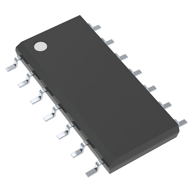
CD4013BCM Description
CD4013BCM Description
The CD4013BCM is a dual D-type flip-flop integrated circuit (IC) designed by onsemi, part of the 4000B series. This IC is well-suited for a variety of digital logic applications due to its robust performance and versatile features. It operates within a wide supply voltage range of 3V to 15V, making it adaptable to different power supply conditions. The CD4013BCM is capable of handling a clock frequency of up to 15.5 MHz, ensuring efficient data processing and synchronization in high-speed digital circuits.
CD4013BCM Features
- Dual D-Type Flip-Flops: The CD4013BCM contains two independent D-type flip-flops, each capable of storing one bit of data. This dual functionality allows for compact and efficient circuit designs.
- Positive Edge Triggering: The flip-flops are triggered on the positive edge of the clock signal, ensuring precise timing and synchronization of data.
- Complementary Outputs: Each flip-flop provides complementary outputs, which can be useful for driving various types of digital circuits and reducing the need for additional inverters.
- Set and Reset Functionality: The CD4013BCM includes set (preset) and reset features, allowing for direct control over the state of the flip-flops. This can be particularly useful in applications requiring initialization or error recovery.
- Low Power Consumption: With a quiescent current of only 4 µA, the CD4013BCM is highly energy-efficient, making it suitable for battery-powered and low-power applications.
- Wide Operating Voltage Range: The IC operates within a wide voltage range of 3V to 15V, providing flexibility in power supply requirements.
- High Output Current Capability: The CD4013BCM can source and sink up to 8.8 mA, enabling it to drive a variety of digital loads directly.
- Low Input Capacitance: The input capacitance of 5 pF ensures minimal loading on the driving circuit, allowing for faster signal propagation.
- Surface Mount Packaging: The CD4013BCM is available in a surface mount package, facilitating easy integration into modern PCB designs.
- Moisture Sensitivity Level 1: The IC is classified as MSL 1, indicating it is not moisture-sensitive and can be stored and handled without special precautions.
CD4013BCM Applications
The CD4013BCM is ideal for a wide range of digital logic applications, including:
- Data Storage and Synchronization: The dual D-type flip-flops can be used to store and synchronize data in digital systems, ensuring reliable data transfer and processing.
- Frequency Division: The flip-flops can be configured to divide clock frequencies, which is useful in applications requiring lower frequency signals.
- Counter Circuits: The set and reset features make the CD4013BCM suitable for building counter circuits, where precise control over the state of the flip-flops is necessary.
- Sequential Logic Circuits: The IC can be used to implement various sequential logic functions, such as state machines and shift registers.
- Digital Signal Processing: The high clock frequency and low propagation delay make the CD4013BCM suitable for applications involving digital signal processing and high-speed data handling.
Conclusion of CD4013BCM
The CD4013BCM is a versatile and reliable dual D-type flip-flop IC that offers a range of features and benefits for digital logic applications. Its wide operating voltage range, low power consumption, and high output current capability make it suitable for a variety of use cases. The positive edge triggering and complementary outputs ensure precise timing and efficient circuit design. While the CD4013BCM is currently marked as obsolete, its robust performance and unique features continue to make it a valuable component for engineers and designers in the electronics industry.
FAQ
Not available to buy online? Want the lower wholesale price? Please Send RFQ to get best price, we will respond immediately


.png?x-oss-process=image/format,webp/resize,h_32)


