
 German
 Japanese
 Portuguese
 Korea
Korea
 Mexico
 Dutch
Dutch


Why Choose Us?
Professional Platform
B2B & B2C purchasingDelivery at full speed
1-2 days deliveryWide variety
Original manufacturers365 days guarantee
Responsible quality
.png)


Tech Specifications
CD4049UBCSJX Description
CD4049UBCSJX Description
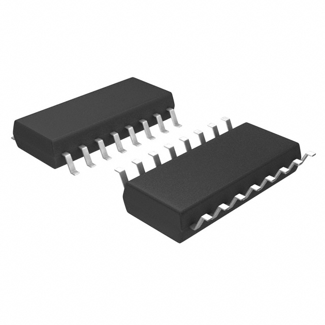
The CD4049UBCSJX is a high-performance inverter logic IC chip, part of the 4000B series, manufactured by onsemi. This surface-mount device features six independent inverter circuits, each with a single input, making it ideal for applications requiring multiple inversion operations. The CD4049UBCSJX operates within a wide supply voltage range of 3V to 15V, ensuring compatibility with various power supply systems. It has a maximum propagation delay of 35ns at 15V and a maximum load capacitance of 50pF, providing fast and reliable signal inversion.
CD4049UBCSJX Features
- Logic Type: Inverter
- Number of Circuits: 6
- Number of Inputs per Circuit: 1
- Supply Voltage Range: 3V to 15V
- Input Logic Levels:
- Low: 1V to 3V
- High: 4V to 12V
- Output Current:
- High: 7.2mA
- Low: 29mA
- Max Propagation Delay: 35ns @ 15V, 50pF
- Max Quiescent Current: 4 µA
- Mounting Type: Surface Mount
- Package: Tape & Reel (TR)
- Moisture Sensitivity Level (MSL): 1 (Unlimited)
- ECCN: EAR99
- REACH Status: REACH Unaffected
- HTSUS: 8542.39.0001
- Manufacturer: onsemi
CD4049UBCSJX Applications
The CD4049UBCSJX is well-suited for a variety of applications due to its robust performance and versatile operating conditions. Key applications include:
- Digital Signal Processing: Inverting digital signals in communication systems and data processing units.
- Clock Signal Generation: Creating inverted clock signals for synchronous digital circuits.
- Noise Reduction: Inverting signals to reduce noise and improve signal integrity in mixed-signal systems.
- Level Shifting: Converting logic levels between different voltage domains in multi-voltage systems.
- Control Logic: Implementing inversion logic in control systems for various industrial and consumer electronics.
Conclusion of CD4049UBCSJX
The CD4049UBCSJX is a versatile and reliable inverter logic IC chip, offering high performance and compatibility with a wide range of supply voltages. Its low quiescent current and fast propagation delay make it an efficient choice for applications requiring multiple inversion operations. Despite being marked as obsolete, the CD4049UBCSJX remains a valuable component for engineers and designers looking for a dependable inverter solution. Its surface-mount package and moisture sensitivity level of 1 ensure ease of integration and robustness in various environments.
FAQ
Not available to buy online? Want the lower wholesale price? Please Send RFQ to get best price, we will respond immediately


.png?x-oss-process=image/format,webp/resize,h_32)


