
 German
 Japanese
 Portuguese
 Korea
Korea
 Mexico
 Dutch
Dutch


Why Choose Us?
Professional Platform
B2B & B2C purchasingDelivery at full speed
1-2 days deliveryWide variety
Original manufacturers365 days guarantee
Responsible quality
.png)


Tech Specifications
CD4051BCSJX Description
CD4051BCSJX Description
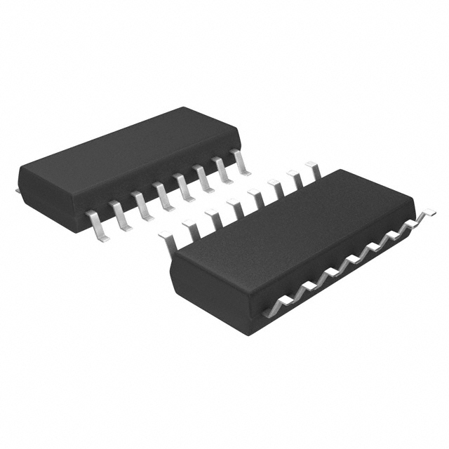
The CD4051BCSJX is an 8:1 multiplexer/demultiplexer integrated circuit (IC) designed for a wide range of analog switching applications. Manufactured by onsemi, this obsolete yet highly reliable component offers exceptional performance with a maximum on-state resistance (Ron) of 240 ohms and a channel-to-channel matching (ΔRon) of 5 ohms. It operates within a dual supply voltage range of ±2.5V to ±7.5V and a single supply voltage range of 5V to 15V, making it versatile for various power configurations. The CD4051BCSJX also boasts a -3dB bandwidth of 40MHz and a maximum switch time of 320ns for turn-on and 150ns for turn-off, ensuring fast and efficient signal routing. With a leakage current (IS(off)) of 50nA, it maintains low power consumption and high signal integrity. Packaged in a surface-mount 16SOP format, it is ideal for compact and high-density designs. The moisture sensitivity level (MSL) of 1 (unlimited) ensures robustness in various environmental conditions.
CD4051BCSJX Features
- Multiplexer/Demultiplexer Circuit: 8:1 configuration allows for efficient signal routing and selection.
- On-State Resistance: Maximum of 240 ohms ensures minimal signal attenuation.
- Channel-to-Channel Matching: ΔRon of 5 ohms provides consistent performance across channels.
- Supply Voltage Range: Dual supply ±2.5V to ±7.5V and single supply 5V to 15V offers flexibility in power configurations.
- Switch Time: Fast turn-on (320ns) and turn-off (150ns) times for rapid signal switching.
- Bandwidth: -3dB bandwidth of 40MHz supports high-frequency applications.
- Leakage Current: Maximum of 50nA ensures low power consumption and high signal integrity.
- Mounting Type: Surface mount in a 16SOP package for compact and high-density designs.
- Moisture Sensitivity Level: MSL 1 (unlimited) ensures reliability in diverse environments.
- REACH Status: REACH unaffected, ensuring compliance with environmental regulations.
CD4051BCSJX Applications
The CD4051BCSJX is ideal for a variety of applications requiring efficient signal routing and selection. Its versatile supply voltage range and high bandwidth make it suitable for:
- Data Acquisition Systems: Efficiently routes multiple analog signals to a single ADC.
- Audio Signal Processing: Switches between different audio inputs with minimal signal degradation.
- Medical Equipment: Ensures reliable signal routing in compact and high-density designs.
- Telecommunications: Provides fast and efficient signal switching in communication systems.
- Industrial Control Systems: Routes multiple sensor signals to a central processing unit.
Conclusion of CD4051BCSJX
The CD4051BCSJX is a robust and versatile 8:1 multiplexer/demultiplexer IC that offers exceptional performance and reliability. Its low on-state resistance, fast switch times, and wide bandwidth make it ideal for high-frequency and high-density applications. Despite being obsolete, its features and performance benefits continue to make it a valuable component in various industries. Its compliance with environmental regulations and robustness against moisture further enhance its suitability for diverse applications.
FAQ
Not available to buy online? Want the lower wholesale price? Please Send RFQ to get best price, we will respond immediately


.png?x-oss-process=image/format,webp/resize,h_32)


