
 German
 Japanese
 Portuguese
 Korea
Korea
 Mexico
 Dutch
Dutch


onsemi
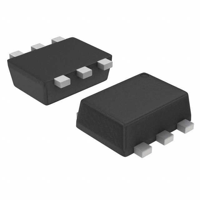
EMT1DXV6T1G

Why Choose Us?
Professional Platform
B2B & B2C purchasingDelivery at full speed
1-2 days deliveryWide variety
Original manufacturers365 days guarantee
Responsible quality
.png)


Tech Specifications
EMT1DXV6T1G Description
EMT1DXV6T1G Description
The EMT1DXV6T1G is a high-performance, dual PNP bipolar transistor array designed and manufactured by onsemi. This device is specifically engineered for applications requiring high-frequency signal amplification and switching. With a maximum collector-emitter breakdown voltage of 60V and a maximum collector current of 100mA, the EMT1DXV6T1G is well-suited for a wide range of electronic systems.
EMT1DXV6T1G Features
- High-Frequency Performance: The EMT1DXV6T1G boasts a transition frequency of 140MHz, making it ideal for high-speed switching and amplification applications.
- Low Saturation Voltage: With a maximum Vce saturation of 500mV at 5mA and 50mA, this device ensures efficient power management and low power dissipation.
- Robust Current Handling: Capable of handling up to 100mA of collector current, the EMT1DXV6T1G is suitable for applications requiring substantial current drive.
- Surface Mount Technology: Designed for surface mount applications, this transistor array simplifies the manufacturing process and enhances reliability.
- Compliance and Certification: The EMT1DXV6T1G is EAR99 and REACH unaffected, ensuring compliance with international trade and environmental regulations.
- DC Current Gain: With a minimum hFE of 120 at 1mA and 6V, this device offers consistent performance across a range of operating conditions.
EMT1DXV6T1G Applications
The EMT1DXV6T1G is an excellent choice for various applications due to its high-frequency capabilities and robust performance:
- RF Amplification: Ideal for use in radio frequency applications where high-frequency signal amplification is required.
- Switching Circuits: The low saturation voltage makes it suitable for power switching applications, ensuring efficient operation.
- Automotive Electronics: With its ability to handle high voltages and currents, the EMT1DXV6T1G is well-suited for automotive electronics, such as ignition systems and sensor interfaces.
- Industrial Control Systems: Reliable for use in industrial control systems where high switching speeds and voltage handling are critical.
Conclusion of EMT1DXV6T1G
The EMT1DXV6T1G from onsemi stands out as a versatile and high-performing dual PNP bipolar transistor array. Its unique combination of high-frequency capabilities, robust current handling, and low saturation voltage make it an ideal choice for a variety of applications, from RF amplification to high-speed switching circuits. With its compliance with international regulations and its surface mount design, the EMT1DXV6T1G is a reliable and efficient solution for demanding electronic systems.
FAQ
Not available to buy online? Want the lower wholesale price? Please Send RFQ to get best price, we will respond immediately


.png?x-oss-process=image/format,webp/resize,h_32)


