
 German
 Japanese
 Portuguese
 Korea
Korea
 Mexico
 Dutch
Dutch


onsemi
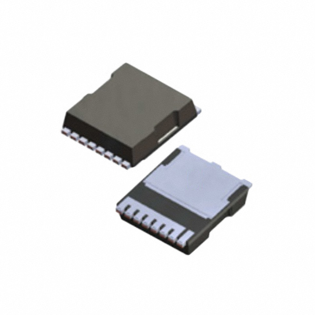
FDBL0200N100

Why Choose Us?
Professional Platform
B2B & B2C purchasingDelivery at full speed
1-2 days deliveryWide variety
Original manufacturers365 days guarantee
Responsible quality
.png)


Tech Specifications
FDBL0200N100 Description
FDBL0200N100 is a MOSFET (Metal-Oxide-Semiconductor Field-Effect Transistor) produced by ON Semiconductor. Here is a brief description of the model along with its features and applications:
Description:
The FDBL0200N100 is an N-channel, logic-level MOSFET in a TO-220 package. It is designed for use in a variety of applications, including low-voltage, low-current switching and amplification.
Features:
- N-Channel, Logic-Level MOSFET
- TO-220 Package
- Low Input and Output Capacitance
- High Switching Speed
- Low On-Resistance (RDS(on))
- Suitable for use in low-voltage, low-current applications
Applications:
- Power Switching
- Motor Control
- DC-DC Converters
- Class-D Audio Amplifiers
- Battery Protection Circuits
- LED Lighting
- General-purpose switching and amplification in low-voltage, low-current applications
Please note that this is a general description of the FDBL0200N100 MOSFET, and you should refer to the datasheet for more detailed information on its specifications, operating conditions, and electrical characteristics.
FAQ
Not available to buy online? Want the lower wholesale price? Please Send RFQ to get best price, we will respond immediately


.png?x-oss-process=image/format,webp/resize,h_32)


