
 German
 Japanese
 Portuguese
 Korea
Korea
 Mexico
 Dutch
Dutch


onsemi
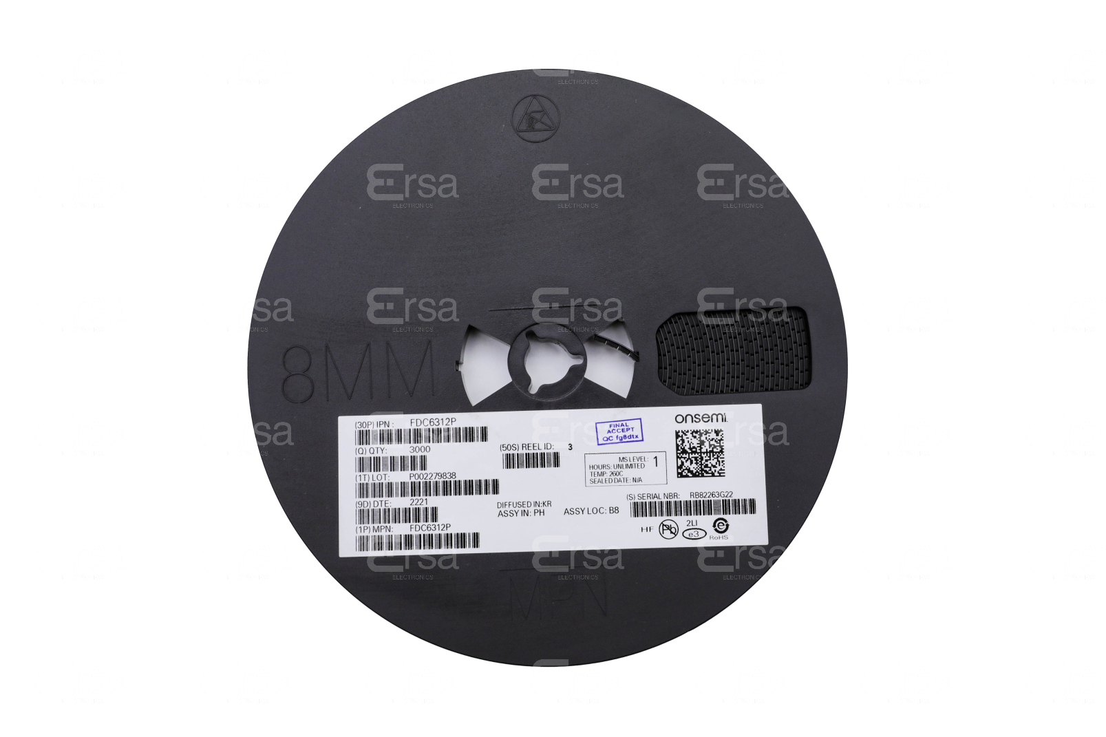
FDC6312P

Why Choose Us?
Professional Platform
B2B & B2C purchasingDelivery at full speed
1-2 days deliveryWide variety
Original manufacturers365 days guarantee
Responsible quality
.png)


Tech Specifications
FDC6312P Description
FDC6312P is a high-performance, single-channel, capacitive touch sensor controller from ON Semiconductor. It is designed to provide a robust and reliable solution for capacitive touch sensing applications in various markets, including consumer electronics, industrial, and automotive.
Description:
The FDC6312P is a highly integrated, low-power touch sensor controller that supports up to 32 touch sensing channels. It features a proprietary scanning algorithm that enables accurate detection and location of touch events, even in noisy environments. The device is available in a compact 24-pin QFN package, making it suitable for space-constrained applications.
Features:
- Single-channel capacitive touch sensor controller
- Supports up to 32 touch sensing channels
- Proprietary scanning algorithm for accurate touch detection
- Wide supply voltage range (2.7V to 5.5V)
- Low power consumption (typical 2.8mA in active mode)
- Configurable touch sensitivity and debounce settings
- I2C and SPI communication interfaces
- On-chip oscillator and clock management
- Small form-factor 24-pin QFN package
Applications:
- Consumer Electronics: Touch-sensitive buttons, sliders, and wheels in smartphones, tablets, and remote controls
- Industrial: Touch-based user interfaces in machinery and equipment
- Automotive: Touch-sensitive controls in dashboards, infotainment systems, and climate control panels
- Appliance Controls: Touch-sensitive buttons and interfaces in home appliances like washing machines, refrigerators, and ovens
- Medical Devices: Touch-based user interfaces in medical equipment and diagnostic devices
- Gaming and Entertainment: Touch-sensitive controls in gaming consoles, arcade machines, and interactive displays
The FDC6312P offers a versatile and efficient solution for capacitive touch sensing applications, providing accurate touch detection and low power consumption in a compact package. Its wide range of features and support for various communication interfaces make it suitable for a broad range of applications across different markets.
FAQ
| Quantity | Unit Price | Ext. Price |
|---|---|---|
| 10+ | $0.52800 | $5.28 |
| 30+ | $0.48000 | $14.40 |
| 100+ | $0.42000 | $42.00 |
| 500+ | $0.39257 | $196.28 |
| 1000+ | $0.37543 | $375.43 |
Not available to buy online? Want the lower wholesale price? Please Send RFQ to get best price, we will respond immediately


.png?x-oss-process=image/format,webp/resize,h_32)


