
 German
 Japanese
 Portuguese
 Korea
Korea
 Mexico
 Dutch
Dutch


onsemi
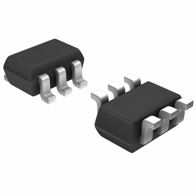
FDG6335N

Why Choose Us?
Professional Platform
B2B & B2C purchasingDelivery at full speed
1-2 days deliveryWide variety
Original manufacturers365 days guarantee
Responsible quality
.png)


Tech Specifications
FDG6335N Description
The FDG6335N is a high-power MOSFET transistor manufactured by ON Semiconductor. It is designed for use in a variety of power electronic applications, including motor control, power supplies, and power converters.
Description:
The FDG6335N is an N-channel MOSFET transistor with a high input impedance, low output impedance, and fast switching capabilities. It features a high voltage rating of 100V and a continuous drain current of 33A. The device is available in a TO-220AB package.
Features:
- N-channel, high-power MOSFET transistor
- High voltage rating of 100V
- Continuous drain current of 33A
- High input impedance and low output impedance
- Fast switching capabilities
- Available in a TO-220AB package
Applications:
The FDG6335N is suitable for use in a variety of power electronic applications, including:
- Motor control
- Power supplies
- Power converters
- Battery management systems
- Inverters
- Switch mode power supplies (SMPS)
- Class D audio amplifiers
Overall, the FDG6335N is a versatile and high-performance MOSFET transistor that can be used in a wide range of power electronic applications. Its high voltage rating, fast switching capabilities, and low output impedance make it an ideal choice for demanding power conversion and control applications.
FAQ
Not available to buy online? Want the lower wholesale price? Please Send RFQ to get best price, we will respond immediately


.png?x-oss-process=image/format,webp/resize,h_32)


