
 German
 Japanese
 Portuguese
 Korea
Korea
 Mexico
 Dutch
Dutch


onsemi
FDL100N50F
278-FDL100N50F

PDF Datasheet
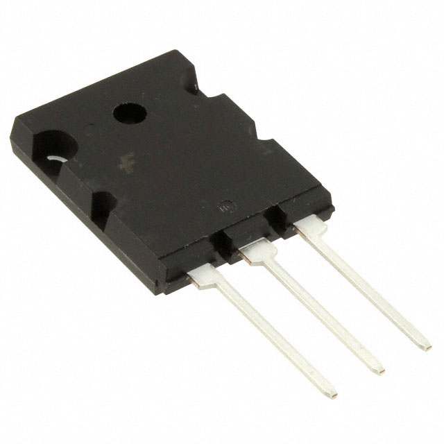
N-Channel MOSFET, 500V, 100A, 55mΩ, TO-264
10 Weeks
Why Choose Us?
Professional Platform
B2B & B2C purchasingDelivery at full speed
1-2 days deliveryWide variety
Original manufacturers365 days guarantee
Responsible quality
.png)


Tech Specifications
Package/Case
TO-264
Continuous Drain Current (ID)
100A
Drain to Source Breakdown Voltage
500V
Drain to Source Resistance
43mR
Drain to Source Voltage (Vdss)
500V
Element Configuration
Single
Fall Time
105ns
Gate to Source Voltage (Vgs)
30V
FDL100N50F Description
N-Channel 500 V 100A (Tc) 2500W (Tc) Through Hole TO-264-3
FAQ
Are there related or alternative parts for FDL100N50F?
Yes. Related or alternative parts may be available on this page when relevant product data is provided.
What is the standard lead time for FDL100N50F?
What operating temperature range does FDL100N50F support?
What is FDL100N50F?
What is the mounting type of FDL100N50F?
Quick Quote
ADD TO RFQ LIST
Not available to buy online? Want the lower wholesale price? Please Send RFQ to get best price, we will respond immediately
QUICK RFQ


.png?x-oss-process=image/format,webp/resize,h_32)


