
 German
 Japanese
 Portuguese
 Korea
Korea
 Mexico
 Dutch
Dutch


onsemi
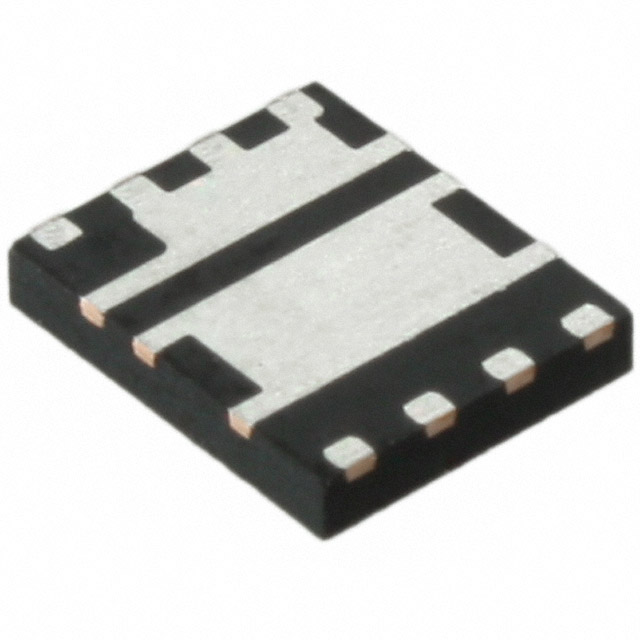
FDMS3660S

Why Choose Us?
Professional Platform
B2B & B2C purchasingDelivery at full speed
1-2 days deliveryWide variety
Original manufacturers365 days guarantee
Responsible quality
.png)


Tech Specifications
FDMS3660S Description
The FDMS3660S is a high voltage, high frequency MOSFET from ON Semiconductor. It is designed for use in a variety of applications, including motor control, power conversion, and power management.
Description:
The FDMS3660S is a N-channel MOSFET with a voltage rating of 100V and a continuous drain current of 9A. It features a low on-state resistance (RDS(on)) of 55mOhm max, which helps to minimize power losses and improve efficiency. The device also has a fast switching speed, with a gate charge (Qg) of 44nC max and a typical switching time of 55ns.
Features:
- 100V, 9A N-channel MOSFET
- Low on-state resistance (RDS(on)) of 55mOhm max
- Fast switching speed with a gate charge (Qg) of 44nC max
- Logic level gate drive for easy integration with microcontrollers
- Avalanche energy rating of 1750mJ
- Built-in body diode for efficient energy transfer in reverse conduction applications
- Available in a compact TO-220 package
Applications:
The FDMS3660S is suitable for a wide range of applications, including:
- Motor control in industrial and automotive systems
- Power conversion and management in battery chargers, power supplies, and inverters
- Switching and regulation in class D audio amplifiers and other high-efficiency power electronics
- Load switching in portable devices and battery-powered equipment
Overall, the FDMS3660S is a versatile and high-performance MOSFET that can help to improve the efficiency and reliability of a wide range of power electronic systems.
FAQ
Not available to buy online? Want the lower wholesale price? Please Send RFQ to get best price, we will respond immediately


.png?x-oss-process=image/format,webp/resize,h_32)


