
 German
 Japanese
 Portuguese
 Korea
Korea
 Mexico
 Dutch
Dutch


onsemi
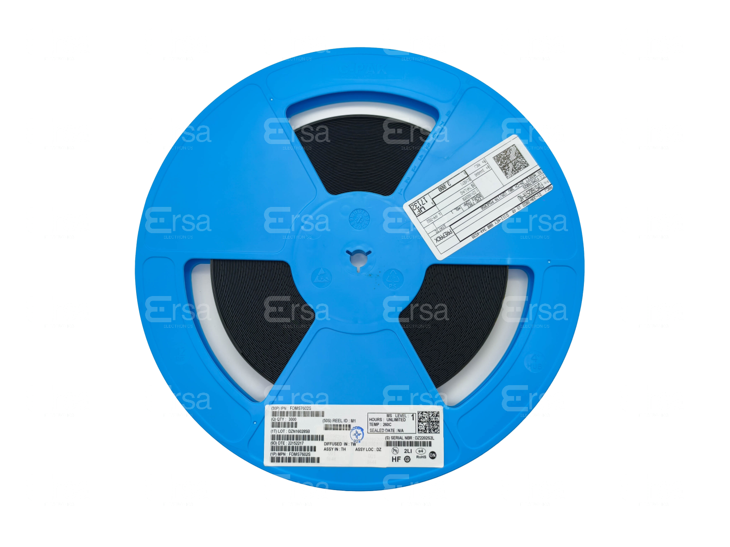
FDMS7602S

Why Choose Us?
Professional Platform
B2B & B2C purchasingDelivery at full speed
1-2 days deliveryWide variety
Original manufacturers365 days guarantee
Responsible quality
.png)


Tech Specifications
FDMS7602S Description
The FDMS7602S is a high-performance, high-power discrete gallium nitride (GaN) transistor from ON Semiconductor. It is designed for use in a wide range of applications, including power conversion, motor drives, and renewable energy systems.
Description:
The FDMS7602S is a normally-off enhancement mode gallium nitride transistor. It features a high breakdown voltage of 100V, a low on-resistance of 65mΩ, and a high input capacitance of 1200pF. The device is available in a compact TO-263-5 package, making it suitable for use in space-constrained applications.
Features:
- High breakdown voltage of 100V
- Low on-resistance of 65mΩ
- High input capacitance of 1200pF
- Normally-off enhancement mode operation
- Suitable for use in a wide range of applications, including power conversion, motor drives, and renewable energy systems
- Available in a compact TO-263-5 package
Applications:
- Power conversion systems, such as AC/DC and DC/DC converters
- Motor drives for industrial and automotive applications
- Renewable energy systems, such as solar power inverters and wind turbine converters
- Class-D audio amplifiers
- High-efficiency power supplies for computing and telecommunications equipment
Overall, the FDMS7602S is a versatile and high-performance GaN transistor that offers excellent electrical characteristics and a compact form factor. Its normally-off enhancement mode operation and low on-resistance make it an ideal choice for a wide range of power conversion and motor drive applications.
FAQ
Not available to buy online? Want the lower wholesale price? Please Send RFQ to get best price, we will respond immediately


.png?x-oss-process=image/format,webp/resize,h_32)


