
 German
 Japanese
 Portuguese
 Korea
Korea
 Mexico
 Dutch
Dutch


Why Choose Us?
Professional Platform
B2B & B2C purchasingDelivery at full speed
1-2 days deliveryWide variety
Original manufacturers365 days guarantee
Responsible quality
.png)


Tech Specifications
FDS6890A Description
The FDS6890A is a high voltage, integrated MOSFET driver from ON Semiconductor. It is designed to drive N-channel MOSFETs in power conversion applications such as motor control, power supplies, and renewable energy systems.
Description:
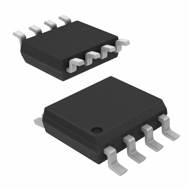
The FDS6890A is a monolithic high voltage MOSFET driver that features a high voltage capability of up to 60V and a peak output current of 2.5A. It is available in a compact SOIC-8 package, making it suitable for space-constrained applications.
Features:
- High voltage capability: The FDS6890A can handle high voltages up to 60V, making it suitable for a wide range of power conversion applications.
- High peak output current: The FDS6890A can provide a peak output current of 2.5A, allowing it to drive large MOSFETs with ease.
- Wide operating temperature range: The FDS6890A can operate over a wide temperature range of -40°C to 125°C, making it suitable for use in harsh environments.
- Logic-level input: The FDS6890A features a logic-level input, allowing it to be easily interfaced with microcontrollers and other digital circuits.
- Undervoltage lockout: The FDS6890A includes an undervoltage lockout feature, which prevents it from operating if the supply voltage falls below a certain threshold.
- Short-circuit protection: The FDS6890A includes short-circuit protection, which helps to protect the MOSFETs from damage in the event of a short circuit.
Applications:
The FDS6890A is suitable for a wide range of power conversion applications, including:
- Motor control: The FDS6890A can be used to drive MOSFETs in brushless DC motor controllers and other motor control applications.
- Power supplies: The FDS6890A can be used to drive MOSFETs in power supply applications such as switched-mode power supplies (SMPS) and battery chargers.
- Renewable energy systems: The FDS6890A can be used to drive MOSFETs in renewable energy systems such as solar inverters and wind turbine converters.
- Industrial control: The FDS6890A can be used to drive MOSFETs in industrial control applications such as robotics and automation systems.
Overall, the FDS6890A is a versatile and high-performance MOSFET driver that is well-suited for a wide range of power conversion applications. Its high voltage capability, high peak output current, and robust protection features make it an excellent choice for driving large MOSFETs in demanding applications.
FAQ
| Quantity | Unit Price | Ext. Price |
|---|---|---|
| 1+ | $1.85828 | $1.86 |
| 10+ | $1.81715 | $18.17 |
| 30+ | $1.79143 | $53.74 |
Not available to buy online? Want the lower wholesale price? Please Send RFQ to get best price, we will respond immediately


.png?x-oss-process=image/format,webp/resize,h_32)


