
 German
 Japanese
 Portuguese
 Korea
Korea
 Mexico
 Dutch
Dutch


onsemi
FOD8342T
906-FOD8342T

PDF Datasheet
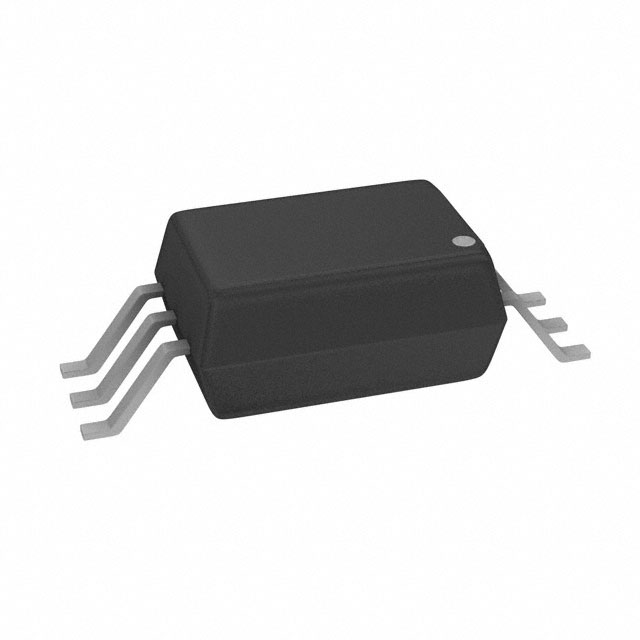
3.0 A Output Current, High Speed Gate Drive Optocouplerin Stretched Body SOP 6-Pin, 2000-TUBE
10 Weeks
Why Choose Us?
Professional Platform
B2B & B2C purchasingDelivery at full speed
1-2 days deliveryWide variety
Original manufacturers365 days guarantee
Responsible quality
.png)


Tech Specifications
Max Operating Temperature
100
Min Operating Temperature
-40
Number of Functions
1
Supply Voltage-Min
10
Number of Elements
1
Eccn Code
EAR99
Lead Free
Yes
HTS Code
8541.40.80.00
FOD8342T Description
3A Gate Driver Optical Coupling 5000Vrms 1 Channel 6-SOP
FAQ
What voltage specification is listed for FOD8342T?
The listed voltage-related specification for FOD8342T is 10.
What is FOD8342T?
What is the standard lead time for FOD8342T?
Are there related or alternative parts for FOD8342T?
Is FOD8342T currently in stock?
Quick Quote
ADD TO RFQ LIST
Not available to buy online? Want the lower wholesale price? Please Send RFQ to get best price, we will respond immediately
QUICK RFQ


.png?x-oss-process=image/format,webp/resize,h_32)


