
onsemi
FSA515UCX
Analog Switches, Multiplexers, Demultiplexers


.png?x-oss-process=image/format,webp/resize,p_30)


FSA515UCX Description
FSA515UCX Description
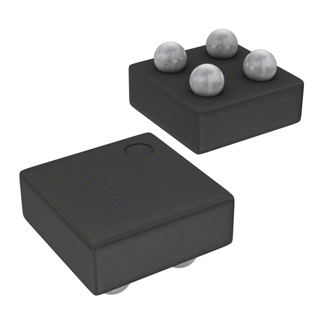
The FSA515UCX is a high-performance analog switch designed and manufactured by onsemi. This 1:1 multiplexer/demultiplexer is specifically engineered for applications requiring low on-state resistance and high bandwidth. With a maximum on-state resistance of 1.1 Ohm and a -3dB bandwidth of 367 MHz, the FSA515UCX delivers exceptional performance in various electronic systems.
FSA515UCX Features
- Low On-State Resistance: The FSA515UCX boasts a maximum on-state resistance of 1.1 Ohm, ensuring minimal signal loss and distortion.
- High Bandwidth: With a -3dB bandwidth of 367 MHz, this switch is ideal for high-speed signal routing and processing applications.
- Low Channel-to-Channel Matching: The FSA515UCX offers excellent channel-to-channel matching with a maximum ΔRon of 1.1 mOhm, minimizing crosstalk and ensuring signal integrity.
- Low Channel Capacitance: The switch features low channel capacitance (CS(off), CD(off)) of 17 pF, reducing signal delay and distortion.
- Fast Switching Times: The FSA515UCX has a typical switch time of 250 µs for Ton and 85 µs for Toff, enabling rapid signal routing.
- Low Leakage Current: The maximum leakage current (IS(off)) is 650 nA, ensuring minimal power consumption and interference in low-power applications.
- RoHS Compliance: The FSA515UCX is RoHS3 compliant, making it suitable for environmentally friendly electronic designs.
- REACH Unaffected: This switch is not affected by REACH regulations, ensuring compliance with European chemical safety standards.
FSA515UCX Applications
The FSA515UCX is ideal for a wide range of applications where high performance, low power consumption, and signal integrity are critical. Some specific use cases include:
- Audio and Video Processing: The low on-state resistance and high bandwidth make it suitable for audio and video signal routing in consumer electronics.
- Telecommunications: The FSA515UCX can be used in high-speed data transmission and signal processing applications in telecommunications systems.
- Industrial Automation: This switch is ideal for signal routing and processing in industrial automation systems, where low power consumption and signal integrity are essential.
- Medical Devices: The low leakage current and high performance make the FSA515UCX suitable for medical devices requiring precise signal processing and low power consumption.
Conclusion of FSA515UCX
The FSA515UCX is a high-performance analog switch that offers a unique combination of low on-state resistance, high bandwidth, and low power consumption. Its excellent channel-to-channel matching and fast switching times make it an ideal choice for a wide range of applications, including audio and video processing, telecommunications, industrial automation, and medical devices. While it is not recommended for new designs, the FSA515UCX remains a reliable and high-performing solution for existing systems that require its specific features.
Tech Specifications
FSA515UCX Documents
Download datasheets and manufacturer documentation for FSA515UCX
 Cancelation of IPCN25081X 02/Oct/2023
  FSA515
  FSA515
  onsemi RoHS
 Shopping Guide


.png?x-oss-process=image/format,webp/resize,h_32)


