
 German
 Japanese
 Portuguese
 Korea
Korea
 Mexico
 Dutch
Dutch


Why Choose Us?
Professional Platform
B2B & B2C purchasingDelivery at full speed
1-2 days deliveryWide variety
Original manufacturers365 days guarantee
Responsible quality
.png)


Tech Specifications
MC10E167FNR2G Description
MC10E167FNR2G Description
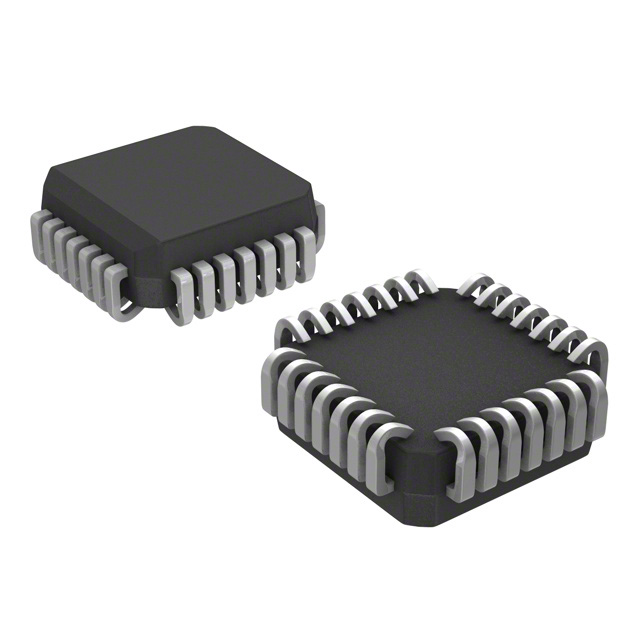
The MC10E167FNR2G is an obsolete, high-performance multiplexer from the 10E series, manufactured by onsemi. This logic IC chip features a 6 x 2:1 multiplexing circuit, designed for surface mount applications. It operates on a dual supply voltage range of ±4.2V to ±5.7V, making it suitable for a variety of electronic systems requiring robust signal routing and switching capabilities. The device is packaged in a 28-pin plastic leaded chip carrier (PLCC) and is available in tape and reel format, facilitating efficient manufacturing processes. Despite its obsolete status, the MC10E167FNR2G remains a reliable choice for specific applications due to its comprehensive feature set and compliance with industry standards such as REACH and ROHS3.
MC10E167FNR2G Features
- Circuit Configuration: The MC10E167FNR2G features a 6 x 2:1 multiplexing circuit, allowing for the selection of one of two input signals for each of the six channels. This configuration provides flexibility in signal routing and switching.
- Dual Supply Voltage: The device operates on a dual supply voltage range of ±4.2V to ±5.7V, ensuring compatibility with a wide range of power supply systems.
- Surface Mount Technology: Designed for surface mount applications, the MC10E167FNR2G is ideal for modern printed circuit board (PCB) designs, offering space efficiency and ease of integration.
- Moisture Sensitivity Level: With a moisture sensitivity level (MSL) of 3 (168 hours), the device is well-suited for manufacturing environments with controlled humidity levels.
- Compliance: The MC10E167FNR2G is REACH unaffected and ROHS3 compliant, ensuring it meets environmental and safety standards for electronic components.
- Packaging: Available in tape and reel (TR) packaging, the device is optimized for automated assembly processes, enhancing manufacturing efficiency.
MC10E167FNR2G Applications
The MC10E167FNR2G is ideal for applications requiring efficient signal routing and switching. Its 6 x 2:1 multiplexing capability makes it suitable for:
- Telecommunications: Switching between multiple data channels in communication systems.
- Data Acquisition Systems: Routing signals from various sensors to a central processing unit.
- Automotive Electronics: Managing signals in complex automotive control systems.
- Industrial Control Systems: Switching between different control signals in industrial automation.
- Medical Equipment: Routing signals in diagnostic and monitoring devices.
Conclusion of MC10E167FNR2G
The MC10E167FNR2G, despite being obsolete, remains a reliable and versatile multiplexer for applications requiring efficient signal routing and switching. Its dual supply voltage range, surface mount design, and compliance with industry standards make it a suitable choice for a variety of electronic systems. While newer alternatives may offer enhanced features, the MC10E167FNR2G continues to provide robust performance and reliability in specific use cases.
FAQ
Not available to buy online? Want the lower wholesale price? Please Send RFQ to get best price, we will respond immediately


.png?x-oss-process=image/format,webp/resize,h_32)


