
 German
 Japanese
 Portuguese
 Korea
Korea
 Mexico
 Dutch
Dutch


onsemi
MC10E451FNR2G

Why Choose Us?
Professional Platform
B2B & B2C purchasingDelivery at full speed
1-2 days deliveryWide variety
Original manufacturers365 days guarantee
Responsible quality
.png)


Tech Specifications
MC10E451FNR2G Description
MC10E451FNR2G Description
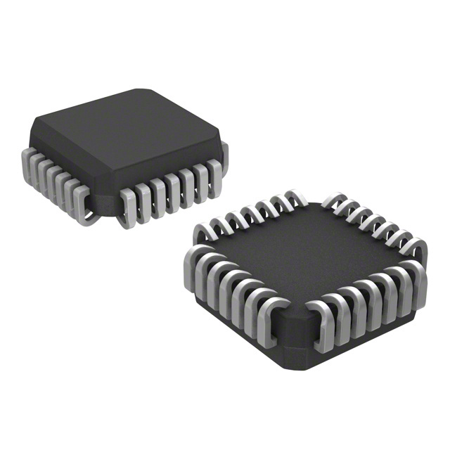
The MC10E451FNR2G is a D-type flip-flop IC designed for high-performance applications requiring robust and reliable data handling. Manufactured by onsemi, this single-element flip-flop operates at a clock frequency of 1.1 GHz, ensuring rapid data processing and synchronization. The device is housed in a 28-pin PLCC package, making it suitable for surface mount technology (SMT) applications. It features a quiescent current of 101 mA, which balances performance with power efficiency. The operating temperature range of 0°C to 85°C (TA) ensures stability and reliability across a wide range of environmental conditions.
MC10E451FNR2G Features
- High Clock Frequency: The 1.1 GHz clock frequency enables the MC10E451FNR2G to handle high-speed data processing, making it ideal for applications requiring rapid data synchronization.
- Single Element with 6 Bits per Element: This configuration allows for efficient data handling and storage, with each flip-flop capable of managing 6 bits of information.
- Positive Edge Triggering: The positive edge-triggered design ensures reliable data capture on each rising edge of the clock signal, minimizing timing errors and improving overall system performance.
- Surface Mount Compatibility: The surface mount mounting type and 28-pin PLCC package make the MC10E451FNR2G suitable for modern PCB designs, facilitating compact and efficient circuit layouts.
- Moisture Sensitivity Level 3: With an MSL rating of 3 (168 hours), the device is well-suited for environments with varying humidity levels, ensuring long-term reliability and performance.
- Compliance and Status: The MC10E451FNR2G is classified under ECCN EAR99 and is REACH unaffected, ensuring compliance with international regulations and standards.
MC10E451FNR2G Applications
The MC10E451FNR2G is designed for a variety of high-speed digital applications where reliable data handling and synchronization are critical. Its high clock frequency and positive edge-triggering make it particularly suitable for:
- Digital Signal Processing: Efficiently synchronizing and processing digital signals in high-speed communication systems.
- Data Storage and Management: Managing data storage operations in systems requiring rapid read/write capabilities.
- Clock and Data Recovery: Ensuring accurate clock signal recovery and data synchronization in digital communication systems.
- High-Speed Counters and Timers: Providing precise timing and counting functions in digital circuits.
Conclusion of MC10E451FNR2G
The MC10E451FNR2G is a versatile and high-performance D-type flip-flop IC that offers significant advantages over similar models. Its 1.1 GHz clock frequency, positive edge-triggering, and surface mount compatibility make it an excellent choice for high-speed digital applications. Despite being marked as obsolete, the MC10E451FNR2G remains a reliable option for engineers and designers seeking a robust and efficient flip-flop solution. Its compliance with international regulations and standards ensures that it can be integrated into modern electronic systems without concerns about regulatory issues.
FAQ
Not available to buy online? Want the lower wholesale price? Please Send RFQ to get best price, we will respond immediately


.png?x-oss-process=image/format,webp/resize,h_32)


