
 German
 Japanese
 Portuguese
 Korea
Korea
 Mexico
 Dutch
Dutch


onsemi
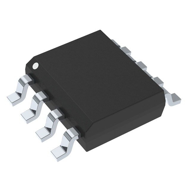
MC33178DR2G

Why Choose Us?
Professional Platform
B2B & B2C purchasingDelivery at full speed
1-2 days deliveryWide variety
Original manufacturers365 days guarantee
Responsible quality
.png)


Tech Specifications
MC33178DR2G Description
The MC33178DR2G is a highly integrated, high-efficiency step-down (buck) regulator from ON Semiconductor. It is designed to provide a compact and efficient solution for power conversion in a wide range of applications.
Description:
The MC33178DR2G is a step-down regulator that converts an input voltage to a lower output voltage. It features a high-efficiency synchronous buck topology and is capable of delivering up to 2A of continuous output current. The device is available in a small, thermally-optimized QFN package, making it well-suited for space-constrained applications.
Features:
- High-efficiency synchronous buck topology with up to 93% efficiency
- Wide input voltage range of 4.75V to 28V
- Output voltage as low as 0.9V
- Capable of delivering up to 2A of continuous output current
- Integrated high-side and low-side MOSFETs
- Programmable soft-start and power-good functions
- Over-current, over-voltage, and thermal protection
- Small, thermally-optimized QFN package
Applications:
The MC33178DR2G is suitable for a wide range of applications that require efficient power conversion, including:
- Portable devices, such as smartphones, tablets, and wearables
- Automotive applications, such as infotainment systems and power mirrors
- Industrial control systems and motor drives
- Telecommunications equipment, such as routers and base stations
- Medical devices, such as hearing aids and portable ultrasound machines
In summary, the MC33178DR2G is a high-efficiency step-down regulator that offers a compact and efficient solution for power conversion in a wide range of applications. Its high efficiency, wide input voltage range, and programmable features make it an ideal choice for designers looking to optimize power conversion in their designs.
FAQ
Not available to buy online? Want the lower wholesale price? Please Send RFQ to get best price, we will respond immediately


.png?x-oss-process=image/format,webp/resize,h_32)


