
onsemi
MM74HC595MTC
Shift Registers


.png?x-oss-process=image/format,webp/resize,p_30)


MM74HC595MTC Description
MM74HC595MTC Description
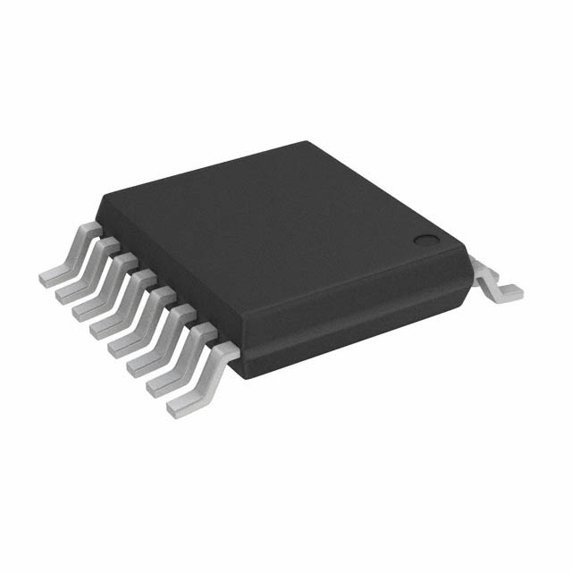
The MM74HC595MTC is an 8-bit shift register with a storage register and 3-state output register, designed for serial-to-parallel data conversion. This device is part of the 74HC series, known for its high-speed CMOS technology. It features an 8-bit serial input shift register, an 8-bit storage register, and 8-bit 3-state outputs. The shift register has a serial input (DS), a serial output (Q7S) for cascading, and a shift register clock input (SH_CP). The storage register has a latch enable input (LE) and 8 outputs (Q0-Q7). The device operates over a supply voltage range of 2V to 6V, making it suitable for a wide range of applications.
MM74HC595MTC Features
- 8-bit Shift Register: The MM74HC595MTC includes an 8-bit shift register that allows data to be shifted in serially and then latched into the storage register.
- Storage Register: The storage register holds the data from the shift register and can be latched using the latch enable (LE) input.
- 3-State Outputs: The device features 8-bit 3-state outputs, which can be enabled or disabled using the output enable (OE) input.
- Wide Operating Voltage Range: The MM74HC595MTC operates over a wide voltage range of 2V to 6V, providing flexibility in power supply requirements.
- Surface Mount Packaging: The device is available in a surface mount package, making it suitable for compact and high-density designs.
- Compliance and Standards: The MM74HC595MTC is REACH unaffected and RoHS3 compliant, ensuring it meets environmental and safety standards.
- Moisture Sensitivity Level: With an MSL of 1 (unlimited), the device is suitable for a variety of manufacturing environments without the need for special handling.
MM74HC595MTC Applications
The MM74HC595MTC is ideal for applications requiring serial-to-parallel data conversion and control of multiple outputs. Some specific use cases include:
- LED Drivers: The device can be used to control multiple LEDs in displays and indicators, providing a compact and efficient solution for lighting control.
- Segment Displays: The MM74HC595MTC can drive segment displays, such as those found in digital clocks and calculators, simplifying the control circuitry.
- Microcontroller Interfaces: The shift register can be used to expand the number of output lines from a microcontroller, allowing for control of multiple devices with fewer I/O pins.
- Data Communication: The device can be used in data communication systems where data needs to be shifted in and out serially, providing a reliable and efficient solution.
Conclusion of MM74HC595MTC
The MM74HC595MTC is a versatile and reliable 8-bit shift register with storage and 3-state output registers, designed for a wide range of applications. Its wide operating voltage range, surface mount packaging, and compliance with environmental standards make it a preferred choice for modern electronic designs. The device's ability to control multiple outputs with a single serial input makes it an efficient solution for applications such as LED drivers, segment displays, and microcontroller interfaces. The MM74HC595MTC is an excellent choice for engineers looking for a robust and flexible shift register solution in their designs.
Tech Specifications
MM74HC595MTC Documents
Download datasheets and manufacturer documentation for MM74HC595MTC
Shopping Guide


.png?x-oss-process=image/format,webp/resize,h_32)


