
 German
 Japanese
 Portuguese
 Korea
Korea
 Mexico
 Dutch
Dutch


onsemi
MOCD217VM
903-MOCD217VM

PDF Datasheet
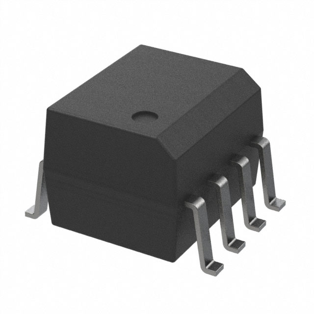
Dual-Channel Phototransistor Optocoupler, 2.5kV Isolation, SOIC
13 Weeks
Why Choose Us?
Professional Platform
B2B & B2C purchasingDelivery at full speed
1-2 days deliveryWide variety
Original manufacturers365 days guarantee
Responsible quality
.png)


Tech Specifications
Package/Case
SOIC
Collector Emitter Saturation Voltage
400mV
Collector Emitter Voltage (VCEO)
400mV
Collector-emitter Voltage-Max
400mV
Current Transfer Ratio
130%
Forward Current
60mA
Input Type
DC
Isolation Voltage
2.5kV
MOCD217VM Description
Optoisolator Transistor Output 2500Vrms 2 Channel 8-SOIC
FAQ
Is MOCD217VM currently in stock?
Yes. MOCD217VM currently shows 525 unit(s) in stock.
Are there related or alternative parts for MOCD217VM?
What operating temperature range does MOCD217VM support?
What is the mounting type of MOCD217VM?
What voltage specification is listed for MOCD217VM?
Quick Quote
ADD TO RFQ LIST
Not available to buy online? Want the lower wholesale price? Please Send RFQ to get best price, we will respond immediately
QUICK RFQ


.png?x-oss-process=image/format,webp/resize,h_32)


