
 German
 Japanese
 Portuguese
 Korea
Korea
 Mexico
 Dutch
Dutch


onsemi
NB100LVEP56MNR2G

Why Choose Us?
Professional Platform
B2B & B2C purchasingDelivery at full speed
1-2 days deliveryWide variety
Original manufacturers365 days guarantee
Responsible quality
.png)


Tech Specifications
NB100LVEP56MNR2G Description
NB100LVEP56MNR2G Description
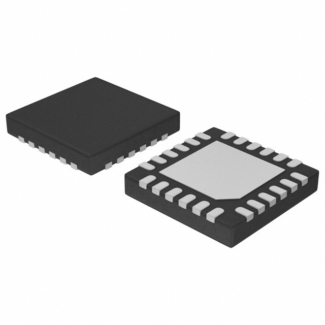
The NB100LVEP56MNR2G is a Differential Digital Multiplexer from onsemi, designed for high-performance signal routing applications. This device is part of the 100LVEP series and features a 2 x 2:1 circuit configuration, making it ideal for applications requiring efficient signal switching. The NB100LVEP56MNR2G is housed in a 24QFN package and is available in a Tape & Reel (TR) format, ensuring ease of integration into surface-mount designs.
NB100LVEP56MNR2G Features
- Circuit Configuration: The NB100LVEP56MNR2G features a 2 x 2:1 circuit configuration, allowing for the selection of two input signals to be routed to a single output. This configuration is highly efficient for applications requiring multiple signal paths.
- Voltage Supply: The device operates on a dual supply voltage ranging from ±2.375V to ±3.8V, providing flexibility in power supply options and ensuring compatibility with a wide range of systems.
- Mounting Type: Surface mount technology (SMT) is utilized, enabling compact and reliable integration into modern electronic designs.
- Product Status: Although the NB100LVEP56MNR2G is marked as obsolete, it remains a robust solution for legacy systems and specific applications where its unique features are required.
- Compliance: The NB100LVEP56MNR2G is REACH unaffected and ROHS3 compliant, ensuring it meets the stringent environmental and safety standards of the electronics industry.
- Moisture Sensitivity Level (MSL): With an MSL rating of 1 (Unlimited), the device is highly resistant to moisture, making it suitable for a wide range of operating environments.
NB100LVEP56MNR2G Applications
The NB100LVEP56MNR2G is ideal for applications requiring high-speed signal switching and efficient signal routing. Its differential digital multiplexer design makes it particularly suitable for:
- Telecommunications: High-speed data routing and signal switching in communication systems.
- Industrial Automation: Efficient signal management in automated control systems.
- Medical Equipment: Reliable signal routing in medical imaging and diagnostic devices.
- Consumer Electronics: Signal switching in high-definition video and audio systems.
Conclusion of NB100LVEP56MNR2G
The NB100LVEP56MNR2G from onsemi is a versatile and reliable differential digital multiplexer, offering unique features and benefits over similar models. Its 2 x 2:1 circuit configuration, dual supply voltage range, and surface mount packaging make it an excellent choice for a variety of applications. Despite its obsolete status, the NB100LVEP56MNR2G remains a valuable component for legacy systems and specific applications where its robust performance and compliance with industry standards are essential.
FAQ
Not available to buy online? Want the lower wholesale price? Please Send RFQ to get best price, we will respond immediately


.png?x-oss-process=image/format,webp/resize,h_32)


