

onsemi
NB3N502DR2G
Clock Generators & Support Products
Not available to buy online? Want the lower wholesale price? Please Send RFQ to get best price, we will respond immediately


.png?x-oss-process=image/format,webp/resize,p_30)


NB3N502DR2G Description
NB3N502DR2G Description
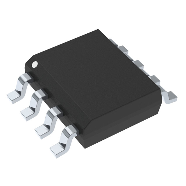
The NB3N502DR2G from onsemi is a high-performance PLL-based clock multiplier IC designed for precision timing applications. This 1:2 ratio clock generator supports input frequencies up to 190MHz and operates within a 3V to 5.5V supply range, making it versatile for mixed-voltage systems. It accepts clock or crystal inputs and delivers CMOS/TTL-compatible outputs, ensuring compatibility with a wide range of digital logic. Housed in an 8-pin SOIC package, it is optimized for surface-mount applications and is available in tape-and-reel (TR) packaging for automated assembly. The device features PLL with bypass capability, allowing flexible clock management, and integrates divider/multiplier functionality for frequency synthesis.
NB3N502DR2G Features
- PLL with Bypass: Enables seamless switching between multiplied or direct clock signals.
- Wide Supply Range (3V–5.5V): Suitable for 3.3V and 5V systems.
- High Frequency (190MHz Max): Ideal for high-speed digital systems.
- 1:2 Input-to-Output Ratio: Doubles input frequency with low jitter.
- CMOS/TTL Outputs: Broad compatibility with logic families.
- Single-Circuit Design: Compact footprint for space-constrained designs.
- RoHS3 Compliant & REACH Unaffected: Meets environmental regulations.
- Industrial-Grade Reliability: MSL 1 (Unlimited) rating for robust handling.
NB3N502DR2G Applications
- Networking Equipment: Clock generation for switches/routers.
- Consumer Electronics: Timing for HDTVs, set-top boxes.
- Embedded Systems: Synchronization in microcontrollers/FPGAs.
- Telecommunications: Frequency synthesis in base stations.
- Automotive Infotainment: Low-jitter clocking for displays/audio.
Conclusion of NB3N502DR2G
The NB3N502DR2G stands out for its flexible PLL architecture, wide voltage support, and high-frequency capability, making it a superior choice for clock distribution in demanding applications. Its small form factor and industry-compliant design ensure easy integration into modern electronics, while features like bypass mode and low-jitter outputs address critical timing challenges. Engineers can leverage this IC for reliable, high-performance clock generation across consumer, industrial, and automotive systems.
Tech Specifications
NB3N502DR2G Documents
Download datasheets and manufacturer documentation for NB3N502DR2G
 NB3N502 Mult MSL1 Pkg Chg 20/Dec/2018 NB3N502 onsemi RoHS onsemi REACH Material Declaration NB3N502DR2G
 Related Parts


Shopping Guide


.png?x-oss-process=image/format,webp/resize,h_32)


©2025 ERSA Electronics Corporation.